BBT3821
2
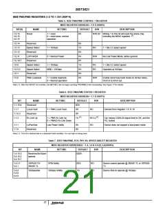
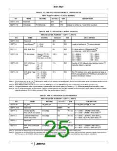
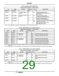
Table 19. I C ONE-BYTE OPERATION WRITE DATA REGISTER
MDIO Register Address = 1.32772 (1.8004’h)
BIT
1.32772.15:8
1.32772.7:0
NAME
Reserved
Write Data
SETTING
DEFAULT
00’h
R/W
RO
R/W
DESCRIPTION
2
I C Write Data
00’h
Data to be written by 1-byte Write Operation
2
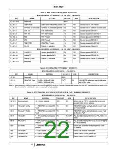
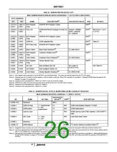
Table 20. NVR I C OPERATION CONTROL REGISTER
MDIO REGISTER ADDRESS = 1.32773 (1.8005’h)
BIT
1.32773.15:9
1.32773.8
NAME
SETTING
DEFAULT
00’h
R/W
RO
DESCRIPTION
Reserved
(1)
2
Long Memory
1 =16 bit
0 = 8 bit
0’b
R/W
R/W
R/W
Length of address for I C device selected
(2)
(3)
1.32773.7
NVR Write Size
0’b
1 = Block write all 256 bytes to NVR
0 = Write only 1.807F:AE’h to NVR
2
2
1.32773.6:4
I C Bus Speed
Speed of I C SCL
100’b
111 = 400kHz
110 = 200kHz
101 = 150kHz
100 = 100kHz
011 = 40kHz
010 = 20kHz
001 = 10kHz
000 = 4kHz
(4)
clock (derived
from REF_CLOCK)
2
1.32773.3:2
1.32773.1:0
NVR ACK Error
Count
11 = 63
10 = 16
01 = 4
00 = 1
11’b
01’b
R/W
R/W
Number of ACK failures at any address before I C
Operation failure is reported
2
NVR Write Page 11 = 32 bytes
(2)
The I C interface block write operation will issue a
STOP and wait for the EEPROM every time after this
number of bytes are sent out
Size
10 = 16 bytes
01 = 8 bytes
00 = 4 byte
2
Note (1): This bit should only be set if an I C device which needs a 16-bit address is to be addressed. The NVR and DOM spaces are all 8-bit address sections, and for
these areas, this bit should be 0’b.
Note (2): Block 256-byte NVR writes will not occur unless the WRTP pin is set Low. NVR Write Page Size controls Page size for Block operations only.
Note (3): This area corresponds to the XENPAK-defined Customer Area; see XENPAK Spec R3.0 Section 10.12.22. Writes will be performed one byte at a time.
2
Note (4): The I C clock speeds listed are approximate. They are derived by division from the CMU, locked to the RFCP/N inputs. At 156.25MHz, the nominal 100kHz
clock will actually be 156.25/1.6kHz, just over 97.5kHz. See also the notes to Table 117.
2
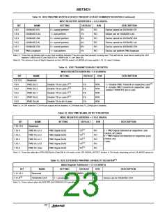
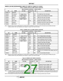
Table 21. NVR I C OPERATION STATUS REGISTER
MDIO REGISTER ADDRESS = 1.32774 (1.8006’h)
BIT
1.32774.15
1.32774.14:4
1.32774.3
NAME
SETTING
XP_ENA pin
DEFAULT
R/W
RO
DESCRIPTION
XP_ENA
1 = XP_ENA pin high, 0 = low
Reserved
0000’h
0’b
RO
Vendor Specific
Area EXOR sum check
Error Flag
Error Flag
RO LH
1 = 1.8106 ! = EXOR(1.80AE:8105)
(2)
0 = 1.8106 = EXOR(1.80AE:8105)
1 = 1.80AD ! = EXOR(1.807E:80AC)
1.32774.2
1.32774.1
1.32774.0
Customer Write Area
EXOR sum check
0’b
0’b
0’b
RO LH
RO
(2)
0 = 1.80AD = EXOR(1.807E:80AC)
Reserved
(1)
LH
NVR Area EXOR sum
check
Error Flag
RO LH
1 = 1.807D ! = EXOR(1.8007:807C)
(2)
0 = 1.807D = EXOR(1.8007:807C)
Note (1): These bits are latched high on any internal error condition detected. They are reset low (cleared) on being read.
Note (2): These bits are set if the EXOR sum calculated from the indicated range is not the same as the value read into the listed checksum register. Note that this is
NOT the same as the XENPAK-defined checksum calculation. Contact Intersil for a method of reconciling these two checksum calculations.
25

 INTERSIL [ Intersil ]