BBT3821
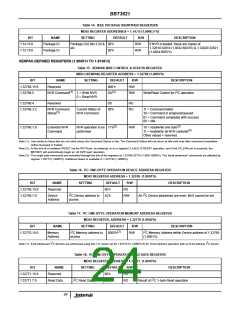
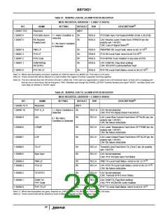
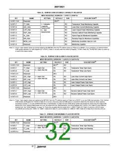
Table 27. XENPAK LASI RX_ALARM STATUS REGISTER
MDIO REGISTER, ADDRESS = 1.36867 (1.9003’h)
(1)
BIT
1.36867.15:6
1.36867.6
1.36867.5
NAME
Reserved
SETTING
DEFAULT
R/W
DESCRIPTION
000’h
PCS Byte Synch 1 = Alarm Condition is 0’b
Detected
RO/LH
RO/LH
PCS Byte Sync Fail (logical NAND of bits 3.24.[3:0])
RX Receive
Power/Level
0’b
LX4: Receive Laser Power from OPRXOP pin (for
polarity see 1.49181)
0 = No Alarm Condition
is Detected
(3)
CX4: Loss of Signal Detect
(2)
1.36867.4
1.36867.3
1.36867.2
1.36867.1
PMA LF
PCS LF
0’b
0’b
0’b
0’b
RO/LH
RO/LH
RO/LH
RO/LH
PMA/PMD RX Local Fault: mirror to bit 1.8.10
(2)
PCS RX Local Fault: mirror to bit 3.8.10
PCS Code
PCS 8b/10b Code Violation in any lane of PCS
DOM RXFlg/
RX EFIFO
LX4: DOM RX_Flag (from polling)
CX4: RX EFIFO over/underflow Fault
(2)
1.36867.0
PHY RX LF
0’b
RO/LH
PHY RX Local Fault Status: mirror to bit 4.8.10
Note (1): Where two descriptions are given, depends on LX4/CX4 select LX4_MODE pin. First value is LX4 value
Note (2): These mirrored bits will be cleared on a read of either this register or of their respective mirroring registers.
Note (3): This bit is derived from the OR of the LOS bits (1.C00A.3:0). In the case of a signal which is close to the LOS threshold value, so that LOS is changing over
time for one or more lanes, this bit may give a “FAIL” indication even though the SIGNAL_DETECT function declares the signal “GOOD”, and Byte Synch and
Lane Align all indicate a “GOOD” signal.
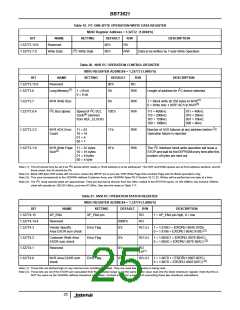
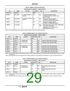
Table 28. XENPAK LASI TX_ALARM STATUS REGISTER
MDIO REGISTER, ADDRESS = 1.36868 (1.9004’h)
(1)
BIT
1.36868.15:11
1.36868.10
NAME
Reserved
SETTING
DEFAULT
000’h
R/W
DESCRIPTION
PHY S_D
1 = Alarm Condition is 0’b
Detected
RO/ LH LX4: No fail detected
CX4: PHY XS Signal Detect Fail (XAUI)
1.36868.9
1.36868.8
1.36868.7
LBC
0’b
RO LH
RO LH
RO LH
LX4: Laser Bias Current Fault (from OPTXLBC pin, for
polarity see 1.49181)
0 = No Alarm
Condition is Detected
CX4: No failure detectable
LTEMP
LOP
0’b
LX4: Laser Temperature Fault (from OPTTEMP pin, for
polarity see 1.49181)
CX4: No failure detectable
0’b
LX4: Laser Output Power Fault (from OPTXLOP pin, for
polarity see 1.49181)
CX4: No failure detectable
1.36868.6
1.36868.5
TX LF
0’b
0’b
RO LH
RO LH
Transmit Local Fault (from TX_FAULT pin, for polarity
see 1.49170)
Byte Sync
LX4: No fail detected
CX4: PHY XS Byte Sync Fail Status
(2)
1.36868.4
1.36868.3
PMA LF
PCS LF
0’b
0’b
RO LH
RO LH
PMA TX Local Fault Status: mirror to bit 1.8.11
(2)
LX4: PCS TX Local Fault Status: mirror to bit 3.8.11
CX4: No failure detectable
1.36868.2
1.36868.1
1.36868.0
TX EFIFO
0’b
0’b
0’b
RO LH
RO LH
RO LH
LX4: No fail detected
CX4: Transmit EFIFO Error Status
DOM TX/
PHY Code
LX4: DOM TX_Flag (from polling)
CX4: PHY XS 8b/10b Code Violation
(2)
PHY TX LF
PHY TX Local Fault Status: mirror to bit 4.8.11
Note (1): Where two descriptions are given, depends on LX4/CX4 select LX4_MODE pin. First value is LX4 value
Note (2): These mirrored bits will be cleared on read of either this register or their respective registers.
28

 INTERSIL [ Intersil ]