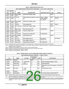
BBT3821
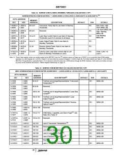
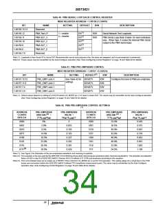
Table 32. XENPAK DOM ALARM & WARNING THRESHOLD REGISTERS COPY
(1)
XENPAK/XPAK/X2 DOM REGISTERS = 1.40960:40999 & 41032:41055 (1.A000:A027’h & A048:A05F’h)
BYTE ADDRESS
DEC HEX
1.40960 to 1.A000 to
MEMORY
ADDRESS
DESCRIPTION
DEFAULT
R/W
RO
DETAILS
00 to 07
08 to15
16 to 23
24 to 31
32-39
Transceiver Temp High & Low Alarm & Warning
Thresholds
Byte Order: High
Alarm MSB:LSB
Low Alarm MSB:LSB
High Warning
MSB:LSB
Low Warning
MSB:LSB
1.40967 1.A007
1.40968 to 1.A008 to
1.40975 1.A00F
Reserved
RO
RO
RO
RO
RO
1.40976 to 1.A010 to
1.40983 1.A017
Laser Bias Current High & Low Alarm & Warning
Thresholds (Lane 0 or common to all lanes)
1.40984 to 1.A018 to
1.40991 1.A01F
Laser Output Power High & Low Alarm &
Warning Thresholds
1.40992to 1.A020 to
1.40099 1.A027
Receive Optical Power High & Low Alarm &
Warning Thresholds
1.41032 to 1.A048 to
1.41055 1.A05F
72 to 95
Lane-by-Lane Laser Bias Current High & Low
Alarm & Warning Thresholds (or Zero)
Order: Lane 1 to
Lane 3
2
Note (1): These1-byte register values are merely copied by the BBT3821 from the I C address space on Power-up or RESET, or on a periodic direct DOM update
operation (i.e. with Register bit 1.C018’h.2 Table 51 not set) under the control of Register 1.A100’h (Table 38). For further details see Table 27 in the XENPAK
MSA Rev 3.0 specification, especially Note 2. If it is desired to write this data into a DOM device through the MDIO interface, it will need to be written one byte
at a time via the methods discussed in “MDIO Register Addressing” on page 15.
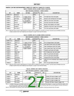
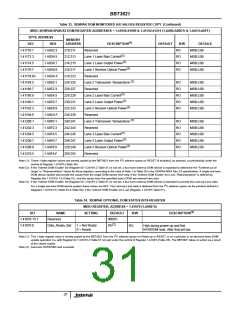
Table 33. XENPAK DOM MONITORED A/D VALUES REGISTER COPY
MDIO XENPAK/XPAK/X2 DOM REGISTER ADDRESSES = 1.41056:41069 & 1.41152:41215 (1.A060:A06D’h & 1.A0C0:A0FF)
BYTE ADDRESS
MEMORY
(1)
DEC
HEX
ADDRESS
DESCRIPTION
DEFAULT
R/W
RO
DETAILS
MSB:LSB
1.41056
1.A060
1.A061
96 & 97
“Farthest out of range/Representative” Transceiver
(2)
1.41057
Temperature
1.41058
1.41059
1.A062
1.A063
98 & 99
Reserved
1.41060
1.41061
1.A064
1.A065
100 & 101
102 & 103
104 & 105
106 to 109
110 to 117
118 to 191
“Farthest out of range/Representative” Laser Bias
RO
RO
RO
MSB:LSB
MSB:LSB
MSB:LSB
(2)
Current
1.41062
1.41063
1.A066
1.A067
“Farthest out of range/Representative” Laser
(2)
Output Power
1.41064
1.41065
1.A068
1.A069
“Farthest out of range/Representative” Receive
(2)
Optical Power
1.41066 -
1.41069
1.A06A to
1.406D
Reserved
(2)
1.41070 to
1.41077
1.A06E to
1.A075
DOM Status, Capability, and Alarm Flags . See
RO
Table 34 to Table 37
1.41078 to
1.41151
1.A076 to
1.A0BF
Reserved
(3)
1.41152:3
1.41154:5
1.41156:7
1.41158:9
1.41160:1
1.41162:7
1.41168:9
1.A0C0:1
1.A0C2:3
1.A0C4:5
1.A0C6:7
1.A0C8:9
1.A0CA:F
1.A0D0:1
192:193
194:195
196:197
198:199
200:201
202:207
208:209
Lane 0 Transceiver Temperature
RO
RO
RO
RO
RO
MSB:LSB
MSB:LSB
MSB:LSB
MSB:LSB
MSB:LSB
Reserved
(3)
Lane 0 Laser Bias Current
(3)
Lane 0 Laser Output Power
(3)
Lane 0 Receive Optical Power
Reserved
(3)
Lane 1 Transceiver Temperature
RO
MSB:LSB
30

 INTERSIL [ Intersil ]