BBT3821
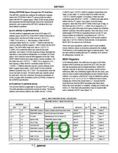
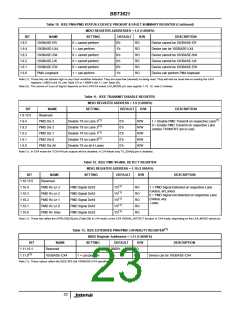
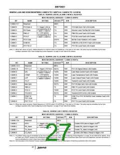
Table 10. IEEE PMA/PMD STATUS 2 DEVICE PRESENT & FAULT SUMMARY REGISTER (Continued)
MDIO REGISTER ADDRESSES = 1.8 (1.0008’h)
BIT
1.8.5
NAME
10GBASE-ER
10GBASE-LX4
10GBASE-SW
10GBASE-LW
10GBASE-EW
PMA Loopback
SETTING
0 = cannot perform
1 = can perform
DEFAULT
0’b
R/W
RO
DESCRIPTION
Device cannot be 10GBASE-ER
Device can be 10GBASE-LX4
Device cannot be 10GBASE-SW
Device cannot be 10GBASE-LW
Device cannot be 10GBASE-EW
Device can perform PMA loopback
1.8.4
1.8.3
1.8.2
1.8.1
1.8.0
1’b
0’b
0’b
0’b
1’b
RO
RO
RO
RO
RO
0 = cannot perform
0 = cannot perform
0 = cannot perform
1 = can perform
Note (1): These bits are latched high on any Fault condition detected. They are reset low (cleared) on being read. They will also be reset low on reading the LASI
registers 1.9003’h (bit 10, see Table 27) or 1.9004’h (bit 11, see Table 28).
Note (2): The source of ‘Loss of Signal’ depends on the LX4/CX4 select LX4_MODE pin (see register 1.10, 12, note (1) below).
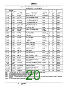
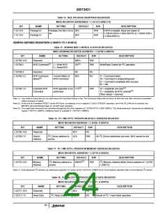
Table 11. IEEE TRANSMIT DISABLE REGISTER
MDIO REGISTER ADDRESS = 1.9 (1.0009’h)
BIT
1.9.15:5
1.9.4
NAME
Reserved
SETTING
DEFAULT
R/W
DESCRIPTION
(1)
(1)
PMD Dis 3
PMD Dis 2
PMD Dis 1
PMD Dis 0
PMD Dis All
Disable TX on Lane 3
Disable TX on Lane 2
Disable TX on Lane 1
Disable TX on Lane 0
0’b
0’b
0’b
0’b
0’b
R/W
1 = Disable PMD Transmit on respective Lane
0 = Enable PMD Transmit on respective Lane
(unless TXON/OFF pin is Low)
(1)
(1)
(1)
1.9.3
R/W
R/W
R/W
R/W
1.9.2
1.9.1
1.9.0
Disable TX on all 4 Lanes
Note (1): In CX4 mode the TCXnP/N pin outputs will be disabled; in LX4 Mode only TX_ENA[n] pin is disabled.
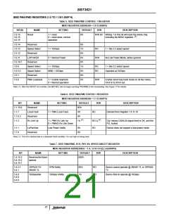
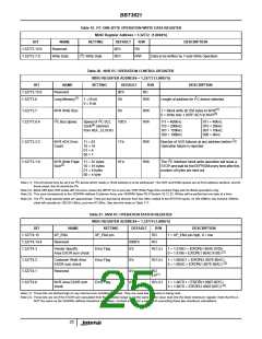
Table 12. IEEE PMD SIGNAL DETECT REGISTER
MDIO REGISTER ADDRESS = 1.10 (1.000A’h)
BIT
1.10.15:5
1.10.4
NAME
Reserved
SETTING
DEFAULT
R/W
DESCRIPTION
(1)
PMD Rx Ln 3
PMD Rx Ln 2
PMD Rx Ln 1
PMD Rx Ln 0
PMD Rx Glob
PMD Signal Det’d
PMD Signal Det’d
PMD Signal Det’d
PMD Signal Det’d
PMD Signal Det’d
1’b
RO
1 = PMD Signal Detected on respective Lane
(Global, all Lanes)
0 = PMD Signal not detected on respective Lane
(1)
(1)
(1)
(1)
1.10.3
1’b
1’b
1’b
1’b
RO
RO
RO
RO
(Global, any
Lane)
1.10.2
1.10.1
1.10.0
Note (1): These bits reflect the OPRLOS[3:0] pins (Table 99) in LX4 mode, or the CX4 SIGNAL_DETECT function in CX4 mode, depending on the LX4_MODE select pin.
(1)
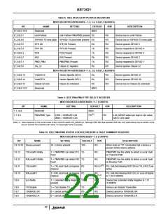
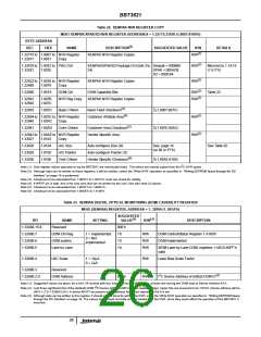
Table 13. IEEE EXTENDED PMA/PMD CAPABILITY REGISTER
MDIO Register Addresses = 1.11 (1.000B’h)
BIT
1.11.15:1
(1)
NAME
Reserved
10GBASE-CX4
SETTING
DEFAULT
0000’h
1’b
R/W
RO
RO
DESCRIPTION
1.11.0
1 = can perform
Device can be 10GBASE-CX4
Note (1): These values reflect the IEEE 802.3ak 10GBASE-CX4 specification.
23

 INTERSIL [ Intersil ]