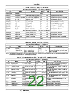
BBT3821
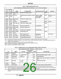
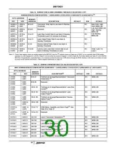
Table 22. XENPAK NVR REGISTER COPY
MDIO XENPAK/XPAK/X2 NVR REGISTER ADDRESSES = 1.32775:33030 (1.8007:8106’h)
BYTE ADDRESS
DEC HEX
1.32775 to 1.8007 to NVR Register
(1)
NAME
DESCRIPTION
SUGGESTED VALUE
R/W
DETAILS
(2)
XENPAK NVR Register Copies
R/W
1.32817 1.8031 Copy
(2)
(2)
1.32818 to 1.8032 to PKG OUI
1.32821 1.8035
XENPAK/XPAK/X2 Package OUI (bits 3 to Xenpak = 0008BE
R/W
R/W
Mirrored to 1.14:15
(1.E:F’h)
24)
XPAK = 000ACB
X2 = 000C64
1.32822 to 1.8036 to NVR Register
XENPAK NVR Register Copies
1.32889
1.8079
Copy
(2)
(2)
1.32890
1.807A
DOM Ctrl
NVR Reg Copy
DOM Capability Bits
R/W
R/W
Table 23
1.32891
1.32892
1.807B
1.807C
XENPAK NVR Register Copies
(3)
1.32893
1.807D
Basic Chksm
Basic Field Checksum
Σ(1.8007:807C)
Σ(1.807E:80AC)
(4)
(2)
(2)
1.32894 to 1.807E to NVR Register
1.32940
Customer Writable Area
R/W
R/W
1.80AC
Copy
(5)
1.32941
1.80AD
Cstm Chksm
Customer Area Checksum
1.32942 to 1.80AE to NVR Register
Vendor Specific Area
1.33027
1.33028
1.33029
1.33030
1.8103
1.8104
1.8105
1.8106
Copy
A/C Size
A/C Pointer
Vndr Chksm
Auto-configure Size (N)
See page 16
(or 00 or FF’h)
See Table 92
Auto-configure Pointer (S)
(6)
Vendor Specific Checksum
Σ(1.80AE:8105)
2
Note (1): Only register values operated on by the BBT3821 are individually listed. The others are merely copied from the I C NVR space.
Note (2): Although data can be written to these registers, it will be volatile, unless the ‘Write NVR’ operation as specified in “Writing EEPROM Space through the I2C
Interface” on page 19 is performed.
Note (3): Checksum to be calculated from 1.8007’h to 1.807C’h. Host can check for validity.
Note (4): If WRTP pin is high, this is the only area that can be written by the user. See also Note (2) above.
Note (5): Checksum to be calculated from 1.807E’h to 1.80AC’h.
Note (6): Checksum to be calculated from 1.80AE’h to 1.8105’h.
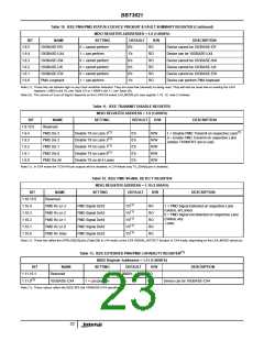
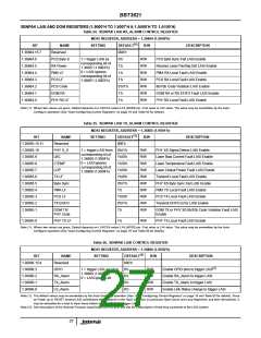
Table 23. XENPAK DIGITAL OPTICAL MONITORING (DOM) CAPABILITY REGISTER
MDIO (XENPAK) REGISTER, ADDRESS = 1. 32890 (1. 807A’h)
SUGGESTED
(1)
(3)
BIT
1.32890.15:8
1.32890.7
1.32890.6
1.32890.5
NAME
Reserved
SETTING
VALUE
000’h
R/W
DESCRIPTION
DOM Ctrl Reg
DOM system
Lane-by Lane
1 = Implemented
0 = Not
implemented
1’b
1’b
1’b
R/W
R/W
R/W
DOM Control/Status Register 1.A100’h
DOM Implemented
WDM Lane-by-Lane DOM; registers 1.A0C0:A0FF’h
valid
1.32890.4
LBC Scale
1 = 10µA
0 = 2µA
R/W
Laser Bias Scale Factor
1.32890.3
Reserved
2
(2)
1.32890.2:0
DOM Address
001’b
R/W
I C Device Address of (initial) DOM IC
Note (1): Suggested values are given, for a full LX4 module with four individual-lane DOM circuits, at least one having the DOM data at Device Address A2’h.
2
Note (2): Last three significant bits of the (default) DOM I C Device Address (NB LSB is a read/write flag). Upper bits are assumed to be ‘1010’b, Device address will be
(A0’h + 2*(<1.32890.2:0>). A device MUST be present at this address for correct operation if bit 6 is set.
Note (3): Although data can be written to this register, it should only be done for writing the NVR, using the ‘Write NVR’ operation as specified in “Writing EEPROM Space
through the I2C Interface” on page 19. The values here should normally only be loaded from the NVR, since they could affect the operation of the BBT3821 if
incorrect.
26

 INTERSIL [ Intersil ]