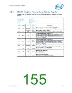
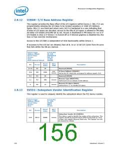
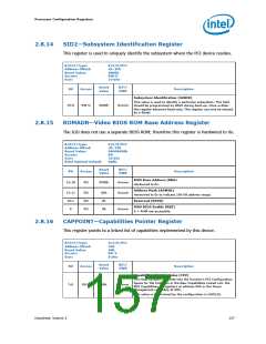
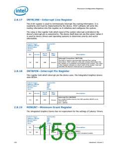
Processor Configuration Registers
2.8.20
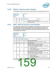
MAXLAT—Maximum Latency Register
The Integrated Graphics Device has no requirement for the settings of Latency Timers.
B/D/F/Type:
Address Offset:
Reset Value:
Access:
0/2/0/PCI
3Fh
00h
RO
8 bits
Size:
Reset
Value
RST/
PWR
Bit
Access
Description
Maximum Latency Value (MLV)
7:0
RO
00h
Uncore
The IGD has no specific requirements for how often it needs to
access the PCI bus.
2.8.21
MSAC—Multi Size Aperture Control Register
This register determines the size of the graphics memory aperture in Function 0 and in
the trusted space. Only the system BIOS will write this register based on pre- boot
address allocation efforts, but the graphics may read this register to determine the
correct aperture size. System BIOS needs to save this value on boot so that it can reset
it correctly during S3 resume.
B/D/F/Type:
Address Offset:
Reset Value:
Access:
0/2/0/PCI
62h
02h
RW, RW-K
8 bits
0h
Size:
BIOS Optimal Default
Reset
Value
RST/
PWR
Bit
Access
Description
Reserved RW (RSVDRW)
7:4
3
RW
RO
0h
0h
Uncore
Uncore
Scratch Bits Only -- Have no physical effect on hardware
Reserved (RSVD)
Untrusted Aperture Size High (LHSASH)
This field is used in conjunction with LHSASL. The description
below is for both fields (LHSASH & LHSASL).
11 = Bits [28:27] of GMADR are RO, allowing 512 MB of GMADR
10 = Illegal Programming
2
RW-K
0b
01 = Bit [28] of GMADR is RW but bit [27] of GMADR is RO,
allowing 256 MB of GMADR
00 = Bits [28:27] of GMADR are RW, allowing 128 MB of GMADR
Untrusted Aperture Size Low (LHSASL)
This field is used in conjunction with LHSASH. The description
below is for both fields (LHSASH & LHSASL).
11 = Bits [28:27] of GMADR are RO, allowing 512 MB of GMADR
10 = Illegal Programming
01 = Bit [28] of GMADR is RW but bit [27] of GMADR is RO,
allowing 256 MB of GMADR
1
0
RW-K
RO
1b
0h
Uncore
00 = Bits [28:27] of GMADR are RW, allowing 128 MB of GMADR
Reserved (RSVD)
Datasheet, Volume 2
159

 INTEL [ INTEL ]