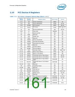
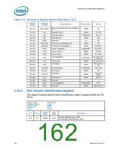
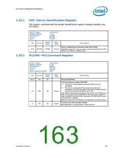
Processor Configuration Registers
2.9
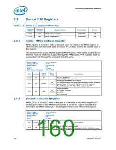
Device 2 IO Registers
Table 2-12. Device 2 IO Register Address Map
Address
Offset
Register
Symbol
Register Name
Reset Value
Access
0–3h
4–7h
Index
Data
MMIO Address Register
MMIO Data Register
00000000h
00000000h
RW
RW
2.9.1
Index—MMIO Address Register
MMIO_INDEX: A 32 bit I/O write to this port loads the offset of the MMIO register or
offset into the GTT that needs to be accessed. An I/O Read returns the current value of
this register.
This mechanism to access internal graphics MMIO registers must not be used to access
VGA I/O registers which are mapped through the MMIO space. VGA registers must be
accessed directly through the dedicated VGA I/O ports.
B/D/F/Type:
Address Offset:
Reset Value:
Access:
0/2/0/PCI IO
0–3h
00000000h
RW
32 bits
00000000h
Size:
BIOS Optimal Default
Reset
Value
RST/
PWR
Bit
Access
Description
31:21
RO
0h
Reserved (RSVD)
Register/GTT Offset (REGGTTO)
This field selects any one of the DWord registers within the MMIO
register space of Device 2 if the target is MMIO Registers.
This field selects a GTT offset if the target is the GTT.
FLR,
20:2
1:0
RW
RW
00000h
00b
Uncore
Target (TARG)
00 = MMIO Registers
01 = GTT
FLR,
Uncore
1X = Reserved
2.9.2
Data—MMIO Data Register
MMIO_DATA: A 32-bit I/O write to this port is re-directed to the MMIO register/GTT
location pointed to by the MMIO-index register. A 32-bit I/O read to this port is re-
directed to the MMIO register/GTT location pointed to by the MMIO-index register.
B/D/F/Type:
Address Offset:
Reset Value:
Access:
0/2/0/PCI IO
4–7h
00000000h
RW
Size:
32 bits
Reset
Value
RST/
PWR
Bit
Access
Description
MMIO Data Window (DATA)
This field is the data field associated with the IO2MMIO access.
FLR,
Uncore
31:0
RW
00000000h
160
Datasheet, Volume 2

 INTEL [ INTEL ]