Processor Configuration Registers
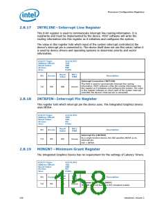
2.8.17
INTRLINE—Interrupt Line Register
This 8-bit register is used to communicate interrupt line routing information. It is
read/write and must be implemented by the device. POST software will write the
routing information into this register as it initializes and configures the system.
The value in this register tells which input of the system interrupt controller(s) the
device's interrupt pin is connected to. The device itself does not use this value; rather it
is used by device drivers and operating systems to determine priority and vector
information.
B/D/F/Type:
Address Offset:
Reset Value:
Access:
0/2/0/PCI
3Ch
00h
RW
8 bits
Size:
Reset
Value
RST/
PWR
Bit
Access
Description
Interrupt Connection (INTCON)
This field is used to communicate interrupt line routing
information. POST software writes the routing information into
this register as it initializes and configures the system. The value
in this register indicates to which input of the system interrupt
controller the device's interrupt pin is connected.
7:0
RW
00h
Uncore
2.8.18
INTRPIN—Interrupt Pin Register
This register tells which interrupt pin the device uses. The Integrated Graphics Device
uses INTA#.
B/D/F/Type:
Address Offset:
Reset Value:
Access:
0/2/0/PCI
3Dh
01h
RO
8 bits
Size:
Reset
Value
RST/
PWR
Bit
Access
Description
Interrupt Pin (INTPIN)
As a single function device, the IGD specifies INTA# as its
interrupt pin.
7:0
RO
01h
Uncore
01h = INTA#.
2.8.19
MINGNT—Minimum Grant Register
The Integrated Graphics Device has no requirement for the settings of Latency Timers.
B/D/F/Type:
Address Offset:
Reset Value:
Access:
0/2/0/PCI
3Eh
00h
RO
8 bits
Size:
Reset
Value
RST/
PWR
Bit
Access
Description
Minimum Grant Value (MGV)
The IGD does not burst as a PCI compliant master.
7:0
RO
00h
Uncore
158
Datasheet, Volume 2

 INTEL [ INTEL ]