LPC Interface Bridge Registers (D31:F0)
Bit
Description
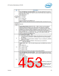
SLP_S3# Minimum Assertion Width: This 2-bit value indicates the minimum
assertion width of the SLP_S3# signal to ensure that the Main power supplies have
been fully power-cycled.
Valid Settings are:
00 = 60–100 us
01 = 1–1.2 ms
11:10
(Corporate
Only)
10 = 50–50.2 ms
11 = 2–2.0002 s
This bit is cleared by the RSMRST# pin.
NOTE: This field is RO when the SLP_Sx# Stretching Policy Lock-Down bit is set.
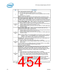
14:10
(Consumer Reserved
Only)
General Reset Status (GEN_RST_STS) — R/WC. This bit is set by hardware
whenever PLTRST# asserts for any reason other than going into a software-
entered sleep state (via PM1CNT.SLP_EN write) or a suspend well power failure
(RSMRST# pin assertion). BIOS is expected to consult and then write a ‘1’ to clear
this bit during the boot flow before determining what action to take based on
PM1_STS.WAK_STS = 1. If GEN_RST_STS = ‘1’, the cold reset boot path should be
followed rather than the resume path, regardless of the setting of WAK_STS.
9
8
This bit is cleared by the RSMRST# pin.
S4_STATE# Pin Disable — R/W.
0 = The traditional SLP_S4# signal (without Intel Management Engine Overrides)
is driven on the S4_STATE# Pin. GPIO26 defaults to its native functionality,
S4_STATE#.
1 = The S4_STATE# pin functionality is disabled. The pin is configured as GPIO26,
default as an output.
NOTE: This bit is cleared by RTCRST#. This bit acts as an override for
GPIO_USE_SEL[26].
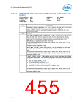
SWSMI_RATE_SEL — R/W. This field indicates when the SWSMI timer will time
out.
Valid values are:
00 = 1.5 ms ± 0.6 ms
7:6
01 = 16 ms ± 4 ms
10 = 32 ms ± 4 ms
11 = 64 ms ± 4 ms
These bits are not cleared by any type of reset except RTCRST#.
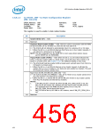
SLP_S4# Minimum Assertion Width — R/W. This field indicates the minimum
assertion width of the SLP_S4# signal to ensure that the DRAMs have been safely
power-cycled.
Valid values are:
11 = 1 to 2 seconds
10 = 2 to 3 seconds
01 = 3 to 4 seconds
00 = 4 to 5 seconds
5:4
This value is used in two ways:
1.
If the SLP_S4# assertion width is ever shorter than this time, a status bit is
set for BIOS to read when S0 is entered.
2.
If enabled by bit 3 in this register, the hardware will prevent the SLP_S4#
signal from deasserting within this minimum time period after asserting.
RTCRST# forces this field to the conservative default state (00b).
NOTE: This field is RO when the SLP_S4# Stretching Policy Lock-Down bit is set.
Datasheet
453

 INTEL [ INTEL ]