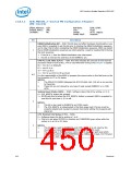
LPC Interface Bridge Registers (D31:F0)
13.8.1.2
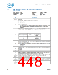
GEN_PMCON_2—General PM Configuration 2 Register
(PM—D31:F0)
Offset Address: A2h
Attribute:
Size:
R/W, R/WC
8-bit
ACPI, Legacy
Resume
Default Value:
Lockable:
00h
No
Usage:
Power Well:
Bit
Description
DRAM Initialization Bit — R/W. This bit does not effect hardware functionality in any
way. BIOS is expected to set this bit prior to starting the DRAM initialization sequence
and to clear this bit after completing the DRAM initialization sequence. BIOS can detect
that a DRAM initialization sequence was interrupted by a reset by reading this bit during
the boot sequence.
7
• If the bit is 1, then the DRAM initialization was interrupted.
• This bit is reset by the assertion of the RSMRST# pin.
CPU PLL Lock Time (CPLT) — R/W. This field indicates the amount of time that the
processor needs to lock its PLLs. This is used wherever timing t270 (Chapter 8) applies.
00 = min 30.7 µs (Default)
01 = min 61.4 µs
10 = min 122.8 µs
11 = min 42 µs (min) to 48 µs (max)
6:5
It is the responsibility of the BIOS to program the correct value in this field prior to the
first transition to C3 or C4 states.
NOTES:
1.
The DPSLP-TO-(G)MCH Message bits (D31:F0:AAh, bits 1:0) act as an override
to these bits.
2.
These bits are not cleared by any type of reset except RSMRST# or a CF9h
write.
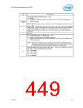
System Reset Status (SRS) — R/WC. Software clears this bit by writing a 1 to it.
0 = SYS_RESET# button Not pressed.
1 = ICH10 sets this bit when the SYS_RESET# button is pressed. BIOS is expected to
read this bit and clear it, if it is set.
4
NOTES:
1.
2.
This bit is also reset by RSMRST# and CF9h resets.
The SYS_RESET# is implemented in the Main power well. This pin must be
properly isolated and masked to prevent incorrectly setting this Suspend well
status bit.
CPU Thermal Trip Status (CTS) — R/WC.
0 = Software clears this bit by writing a 1 to it.
1 = This bit is set when PLTRST# is inactive and THRMTRIP# goes active while the
system is in an S0 or S1 state.
3
NOTES:
1.
This bit is also reset by RSMRST#, and CF9h resets. It is not reset by the
shutdown and reboot associated with the CPUTHRMTRIP# event.
The CF9h reset in the description refers to CF9h type core well reset which
includes SYS_RST#, PWROK/VRMPWRGD low, SMBus hard reset, TCO Timeout.
This type of reset will clear CTS bit.
2.
450
Datasheet

 INTEL [ INTEL ]