LPC Interface Bridge Registers (D31:F0)
13.8
Power Management Registers (PM—D31:F0)
The power management registers are distributed within the PCI Device 31: Function 0
space, as well as a separate I/O range. Each register is described below. Unless
otherwise indicate, bits are in the main (core) power well.
Bits not explicitly defined in each register are assumed to be reserved. When writing to
a reserved bit, the value should always be 0. Software should not attempt to use the
value read from a reserved bit, as it may not be consistently 1 or 0.
13.8.1
Power Management PCI Configuration Registers
(PM—D31:F0)
Table 13-9 shows a small part of the configuration space for PCI Device 31: Function 0.
It includes only those registers dedicated for power management. Some of the
registers are only used for Legacy Power management schemes.
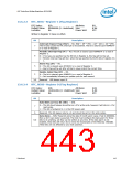
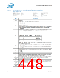
Table 13-9. Power Management PCI Register Address Map (PM—D31:F0)
Offset
Mnemonic
Register Name
Default
Type
General Power Management
Configuration 1
R/W,, R/WO,
RO
A0h
GEN_PMCON_1
0000h
General Power Management
Configuration 2
A2h
A4h
A6h
GEN_PMCON_2
GEN_PMCON_3
00h
00h
00h
R/W, R/WC
R/W, R/WC
RO, R/WLO
General Power Management
Configuration 3
GEN_PMCON_LO General Power Management
CK
Configuration Lock
A9h
AAh
Cx-STATE_CNF
Cx State Configuration
00h
00h
R/W
R/W
C4-TIMING_CNT C4 Timing Control
ABh
BM_BREAK_EN
PMIR
BM_BREAK_EN
00h
R/W
ACh
Power Management Initialization
GPI Route Control
00000000h
00000000h
R/W, R/WL
R/W
B8–BBh
GPI_ROUT
Datasheet
447

 INTEL [ INTEL ]