Chipset Configuration Registers
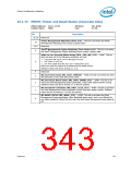
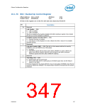
10.1.76 BUC—Backed Up Control Register
Offset Address: 3414–3414h
Default Value: 0000000xb
Attribute:
Size:
R/W
8-bit
All bits in this register are in the RTC well and only cleared by RTCRST#
Bit
Description
7:6
Reserved
LAN Disable — R/W.
0 = LAN is Enabled
1 = LAN is Disabled.
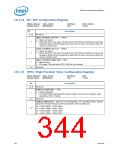
5
This bit is locked by the Function Disable SUS Well Lockdown register. Once locked
this bit can not be changed by software.
Daylight Savings Override (SDO) — R/W.
0 = Daylight Savings is Enabled.
4
3
1 = The DSE bit in RTC Register B is set to Read-only with a value of 0 to disable
daylight savings.
Reserved
CPU BIST Enable (CBE) — R/W. This bit is in the resume well and is reset by
RSMRST#, but not PLTRST# nor CF9h writes.
0 = Disabled.
2
1
1 = The INIT# signals will be driven active when CPURST# is active. INIT# and
INIT3_3V# will go inactive with the same timings as the other processor
interface signals (hold time after CPURST# inactive).
Reserved
Top Swap (TS) — R/W.
0 = Intel® ICH10 will not invert A16.
1 = ICH10 will invert A16 for cycles going to the BIOS space (but not the feature
space) in the FWH.
0
If ICH is strapped for Top-Swap (GNT3# is low at rising edge of PWROK), then this bit
cannot be cleared by software. The strap jumper should be removed and the system
rebooted.
Datasheet
347

 INTEL [ INTEL ]