Chipset Configuration Registers
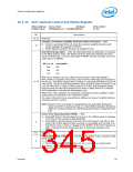
10.1.73 RC—RTC Configuration Register
Offset Address: 3400–3403h
Attribute:
Size:
R/W, R/WLO
32-bit
Default Value:
00000000h
Bit
Description
31:5
4
Reserved
Upper 128 Byte Lock (UL) — R/WLO.
0 = Bytes not locked.
1 = Bytes 38h-3Fh in the upper 128-byte bank of RTC RAM are locked and cannot be
accessed. Writes will be dropped and reads will not return any ensured data. Bit
reset on system reset.
Lower 128 Byte Lock (LL) — R/WLO.
0 = Bytes not locked.
3
1 = Bytes 38h-3Fh in the lower 128-byte bank of RTC RAM are locked and cannot be
accessed. Writes will be dropped and reads will not return any ensured data. Bit
reset on system reset.
Upper 128 Byte Enable (UE) — R/W.
2
0 = Bytes locked.
1 = The upper 128-byte bank of RTC RAM can be accessed.
1:0
Reserved
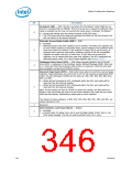
10.1.74 HPTC—High Precision Timer Configuration Register
Offset Address: 3404–3407h
Attribute:
Size:
R/W
32-bit
Default Value:
00000000h
Bit
Description
31:8
Reserved
Address Enable (AE) — R/W.
0 = Address disabled.
7
1 = The Intel® ICH10 will decode the High Precision Timer memory address range
selected by bits 1:0 below.
6:2
Reserved
Address Select (AS) — R/W. This 2-bit field selects 1 of 4 possible memory address
ranges for the High Precision Timer functionality. The encodings are:
00 = FED0_0000h – FED0_03FFh
01 = FED0_1000h – FED0_13FFh
10 = FED0_2000h – FED0_23FFh
11 = FED0_3000h – FED0_33FFh
1:0
344
Datasheet

 INTEL [ INTEL ]