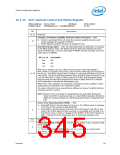
Chipset Configuration Registers
Bit
Description
No Reboot (NR) — R/W. This bit is set when the “No Reboot” strap (SPKR pin on
ICH10) is sampled high on PWROK. This bit may be set or cleared by software if the
strap is sampled low but may not override the strap when it indicates “No Reboot”.
5
0 = System will reboot upon the second timeout of the TCO timer.
1 = The TCO timer will count down and generate the SMI# on the first timeout, but
will not reboot on the second timeout.
Alternate Access Mode Enable (AME) — R/W.
0 = Disabled.
1 = Alternate access read only registers can be written, and write only registers can
be read. Before entering a low power state, several registers from powered down
parts may need to be saved. In the majority of cases, this is not an issue, as
registers have read and write paths. However, several of the ISA compatible
registers are either read only or write only. To get data out of write-only
registers, and to restore data into read-only registers, the ICH implements an
alternate access mode. For a list of these registers see Section 5.13.9.
4
3
Shutdown Policy Select (SPS) — R/W. When cleared (default), the ICH10 will
drive INIT# in response to the shutdown Vendor Defined Message (VDM). When set
to 1, ICH10 will treat the shutdown VDM similar to receiving a CF9h I/O write with
data value06h, and will drive PLTRST# active.
Reserved Page Route (RPR) — R/W. Determines where to send the reserved page
registers. These addresses are sent to PCI or LPC for the purpose of generating POST
codes. The I/O addresses modified by this field are: 80h, 84h, 85h, 86h, 88h, 8Ch,
8Dh, and 8Eh.
0 = Writes will be forwarded to LPC, shadowed within the ICH, and reads will be
returned from the internal shadow
1 = Writes will be forwarded to PCI, shadowed within the ICH, and reads will be
returned from the internal shadow.
2
Note, if some writes are done to LPC/PCI to these I/O ranges, and then this bit is
flipped, such that writes will now go to the other interface, the reads will not return
what was last written. Shadowing is performed on each interface.
The aliases for these registers, at 90h, 94h, 95h, 96h, 98h, 9Ch, 9Dh, and 9Eh, are
always decoded to LPC.
1
0
Reserved
BIOS Interface Lock-Down (BILD) — R/WLO.
0 = Disabled.
1 = Prevents BUC.TS (offset 3414, bit 0) and GCS.BBS (offset 3410h, bits 11:10)
from being changed. This bit can only be written from 0 to 1 once.
346
Datasheet

 INTEL [ INTEL ]