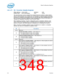
Chipset Configuration Registers
Bit
Description
PCI Express 1 Disable (PE1D) — R/W. Default is 0. When disabled, the link for
this port is put into the link down state.
16
0 = PCI Express port #1 is enabled.
1 = PCI Express port #1 is disabled.
EHCI #1 Disable (EHCI1D) — R/W. Default is 0.
15
14
0 = The EHCI #1 is enabled.
1 = The EHCI #1 is disabled.
LPC Bridge Disable (LBD) — R/W. Default is 0.
0 = The LPC bridge is enabled.
1 = The LPC bridge is disabled. Unlike the other disables in this register, the
following additional spaces will no longer be decoded by the LPC bridge:
•
•
•
· Memory cycles below 16 MB (1000000h)
· I/O cycles below 64 KB (10000h)
· The Internal I/OxAPIC at FEC0_0000 to FECF_FFFF
Memory cycles in the LPC BIOS range below 4 GB will still be decoded when this bit
is set, but the aliases at the top of 1 MB (the E and F segment) no longer will be
decoded.
EHCI #2 Disable (EHCI2D) — R/W. Default is 0.
0 = The EHCI #2 is enabled.
1 = The EHCI #2 is disabled.
13
12
11
Note: When this bit is set, the UHCI #5 function is not available and the UHCI #4
must be disabled by setting bit 11 in this register.
UHCI #5 Disable (U5D) — R/W. Default is 0
0 = The UHCI #5 is enabled.
1 = The UHCI #5 is disabled.
When the EHCI #2 Device Disable (EHCI2D) is set, this bit is a don’t care
UHCI #4 Disable (U4D) — R/W. Default is 0.
0 = The 4th UHCI (ports 6 and 7) is enabled.
1 = The 4th UHCI (ports 6 and 7) is disabled.
Note that UHCI #4 must be disabled when EHCI #2 is disabled with bit 13 in this
register.
UHCI #3 Disable (U3D) — R/W. Default is 0.
10
9
0 = The 3rd UHCI (ports 4 and 5) is enabled.
1 = The 3rd UHCI (ports 4 and 5) is disabled.
UHCI #2 Disable (U2D) — R/W. Default is 0.
0 = The 2nd UHCI (ports 2 and 3) is enabled.
1 = The 2nd UHCI (ports 2 and 3) is disabled.
UHCI #1 Disable (U1D) — R/W. Default is 0.
8
0 = The 1st UHCI (ports 0 and 1) is enabled.
1 = The 1st UHCI (ports 0 and 1) is disabled.
UHCI #6 Disable (U6D) — R/W. Default is 0.
7
0 = The 6th UHCI (ports 10 and 11) is enabled.
1 = The 6th UHCI (ports 10 and 11) is disabled.
USB Test Devices #1 and #2 — R/W. Default is 0.
6:5
(Corporate
Only)
BIOS must set these bits to 11b.
NOTE: These bits only apply to ICH10 Corporate A0, A1, and B0 Samples and are
reserved for ICH10 Corporate Production units.
Datasheet
349

 INTEL [ INTEL ]