DRAM Controller Registers (D0:F0)
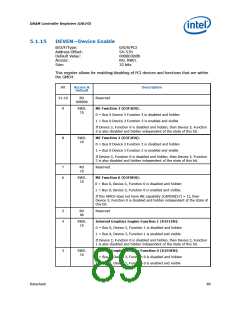
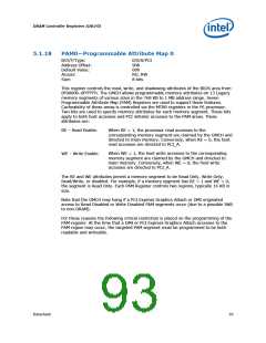
5.1.15
DEVEN—Device Enable
B/D/F/Type:
Address Offset:
Default Value:
Access:
0/0/0/PCI
54–57h
000003DBh
RO, RW/L
32 bits
Size:
This register allows for enabling/disabling of PCI devices and functions that are within
the GMCH.
Bit
31:10
9
Access &
Default
Description
RO
00000h
Reserved
RW/L
1b
ME Function 3 (D3F3EN):
0 = Bus 0 Device 3 Function 3 is disabled and hidden
1 = Bus 0 Device 3 Function 3 is enabled and visible
If Device 3, Function 0 is disabled and hidden, then Device 3, Function
3 is also disabled and hidden independent of the state of this bit.
8
RW/L
1b
ME Function 2 (D3F2EN):
0 = Bus 0 Device 3 Function 2 is disabled and hidden
1 = Bus 0 Device 3 Function 2 is enabled and visible
If Device 3, Function 0 is disabled and hidden, then Device 3, Function
2 is also disabled and hidden independent of the state of this bit.
7
6
RO
1b
Reserved
RW/L
1b
ME Function 0 (D3F0EN):
0 = Bus 0, Device 3, Function 0 is disabled and hidden
1 = Bus 0, Device 3, Function 0 is enabled and visible.
If this GMCH does not have ME capability (CAPID0[57] = 1), then
Device 3, Function 0 is disabled and hidden independent of the state of
this bit.
5
4
RO
0b
Reserved
RW/L
1b
Internal Graphics Engine Function 1 (D2F1EN):
0 = Bus 0, Device 2, Function 1 is disabled and hidden
1 = Bus 0, Device 2, Function 1 is enabled and visible
If Device 2, Function 0 is disabled and hidden, then Device 2, Function
1 is also disabled and hidden independent of the state of this bit.
3
RW/L
1b
Internal Graphics Engine Function 0 (D2F0EN):
0 = Bus 0, Device 2, Function 0 is disabled and hidden
1 = Bus 0, Device 2, Function 0 is enabled and visible
Datasheet
89

 INTEL [ INTEL ]