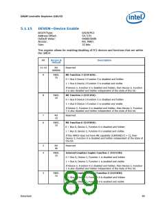
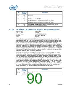
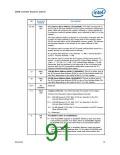
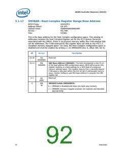
DRAM Controller Registers (D0:F0)
5.1.18
PAM0—Programmable Attribute Map 0
B/D/F/Type:
Address Offset:
Default Value:
Access:
0/0/0/PCI
90h
00h
RO, RW
8 bits
Size:
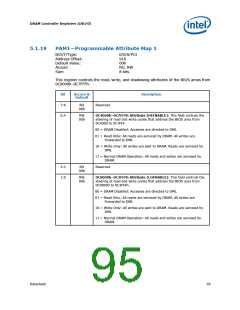
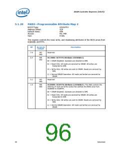
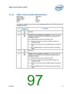
This register controls the read, write, and shadowing attributes of the BIOS area from
0F0000h–0FFFFFh. The GMCH allows programmable memory attributes on 13 Legacy
memory segments of various sizes in the 768 KB to 1 MB address range. Seven
Programmable Attribute Map (PAM) Registers are used to support these features.
Cacheability of these areas is controlled via the MTRR registers in the P6 processor.
Two bits are used to specify memory attributes for each memory segment. These bits
apply to both host accesses and PCI initiator accesses to the PAM areas. These
attributes are:
RE – Read Enable.
When RE = 1, the processor read accesses to the
corresponding memory segment are claimed by the GMCH and
directed to main memory. Conversely, when RE = 0, the host
read accesses are directed to PCI_A.
WE – Write Enable.
When WE = 1, the host write accesses to the corresponding
memory segment are claimed by the GMCH and directed to
main memory. Conversely, when WE = 0, the host write
accesses are directed to PCI_A.
The RE and WE attributes permit a memory segment to be Read Only, Write Only,
Read/Write, or disabled. For example, if a memory segment has RE = 1 and WE = 0,
the segment is Read Only. Each PAM Register controls two regions, typically 16 KB in
size.
Note that the GMCH may hang if a PCI Express Graphics Attach or DMI originated
access to Read Disabled or Write Disabled PAM segments occur (due to a possible IWB
to non-DRAM).
For these reasons the following critical restriction is placed on the programming of the
PAM regions: At the time that a DMI or PCI Express Graphics Attach accesses to the
PAM region may occur, the targeted PAM segment must be programmed to be both
readable and writeable.
Datasheet
93

 INTEL [ INTEL ]