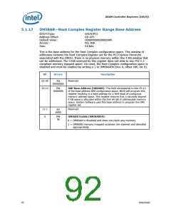
DRAM Controller Registers (D0:F0)
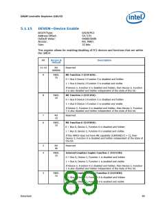
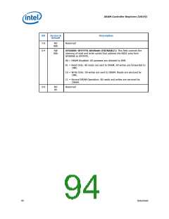
Bit
2
Access &
Default
Description
RO
0b
Reserved
1
RW/L
1b
PCI Express Port (D1EN):
0 = Bus 0, Device 1, Function 0 is disabled and hidden.
1 = Bus 0, Device 1, Function 0 is enabled and visible.
0
RO
1b
Host Bridge (D0EN): Bus 0, Device 0, Function 0 may not be
disabled and is therefore hardwired to 1.
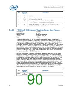
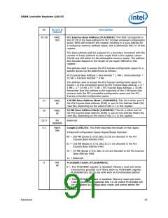
5.1.16
PCIEXBAR—PCI Express* Register Range Base Address
B/D/F/Type:
Address Offset:
Default Value:
Access:
0/0/0/PCI
60–67h
00000000E0000000h
RO, RW/L, RW/L/K
64 bits
Size:
This is the base address for the PCI Express configuration space. This window of
addresses contains the 4 KB of configuration space for each PCI Express device that
can potentially be part of the PCI Express Hierarchy associated with the GMCH. There
is not actual physical memory within this window of up to 256 MB that can be
addressed. The actual length is determined by a field in this register. Each PCI Express
Hierarchy requires a PCI Express BASE register. The GMCH supports one PCI Express
hierarchy. The region reserved by this register does not alias to any PCI 2.3 compliant
memory mapped space. For example, MCHBAR reserves a 16 KB space and CHAPADR
reserves a 4 KB space both outside of PCIEXBAR space. They cannot be overlayed on
the space reserved by PCIEXBAR for devices 0.
On reset, this register is disabled and must be enabled by writing a 1 to the enable
field in this register. This base address shall be assigned on a boundary consistent
with the number of buses (defined by the Length field in this register), above TOLUD
and still within 64 bit addressable memory space. All other bits not decoded are read
only 0. The PCI Express Base Address cannot be less than the maximum address
written to the Top of physical memory register (TOLUD). Software must ensure that
these ranges do not overlap with known ranges located above TOLUD. Software must
ensure that the sum of Length of enhanced configuration region + TOLUD + (other
known ranges reserved above TOLUD) is not greater than the 36-bit addressable limit
of 64 GB. In general system implementation and number of PCI/PCI Express/PCI-X
buses supported in the hierarchy will dictate the length of the region.
Bit
Access &
Default
Description
63:36
RO
Reserved
0000000h
90
Datasheet

 INTEL [ INTEL ]