DRAM Controller Registers (D0:F0)
Bit
Access &
Default
Description
35:28
RW/L
0Eh
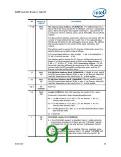
PCI Express Base Address (PCIEXBAR): This field corresponds to
bits 35:28 of the base address for PCI Express enhanced configuration
space. BIOS will program this register resulting in a base address for
a contiguous memory address space; size is defined by bits 2:1 of this
register.
This Base address shall be assigned on a boundary consistent with the
number of buses (defined by the Length field in this register) above
TOLUD and still within 64-bit addressable memory space. The address
bits decoded depend on the length of the region defined by this
register.
The address used to access the PCI Express configuration space for a
specific device can be determined as follows:
PCI Express Base Address + Bus Number * 1 MB + Device Number *
32 KB + Function Number * 4 KB
The address used to access the PCI Express configuration space for
Device 1 in this component would be PCI Express Base Address + 0 *
1 MB + 1 * 32 KB + 0 * 4 KB = PCI Express Base Address + 32 KB.
Remember that this address is the beginning of the 4 KB space that
contains both the PCI compatible configuration space and the PCI
Express extended configuration space.
128 MB Base Address Mask (128ADMSK): This bit is either part of
the PCI Express Base Address (R/W) or part of the Address Mask (RO,
read 0b), depending on the value of bits 2:1 in this register.
27
26
RW/L
0b
64 MB Base Address Mask (64ADMSK): This bit is either part of
the PCI Express Base Address (R/W) or part of the Address Mask (RO,
read 0b), depending on the value of bits 2:1 in this register.
RW/L
0b
25:3
2:1
RO
000000h
Reserved
RW/K
00b
Length (LENGTH): This Field describes the length of this region.
Enhanced Configuration Space Region/Buses Decoded
00 = 256 MB (buses 0–255). Bits 31:28 are decoded in the PCI
Express Base Address Field
01 = 128 MB (Buses 0–127). Bits 31:27 are decoded in the PCI
Express Base Address Field.
10 = 64 MB (Buses 0–63). Bits 31:26 are decoded in the PCI Express
Base Address Field.
11 = Reserved
0
RW
0b
PCIEXBAR Enable (PCIEXBAREN):
0 = The PCIEXBAR register is disabled. Memory read and write
transactions proceed as if there were no PCIEXBAR register.
PCIEXBAR bits 35:26 are R/W with no functionality behind
them.
1 = The PCIEXBAR register is enabled. Memory read and write
transactions whose address bits 31:26 match PCIEXBAR will
be translated to configuration reads and writes within the
GMCH.
Datasheet
91

 INTEL [ INTEL ]