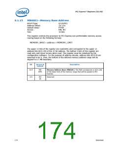
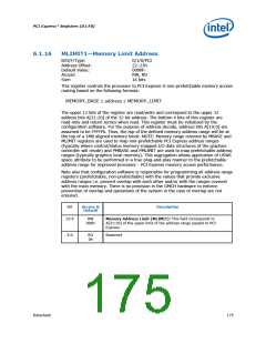
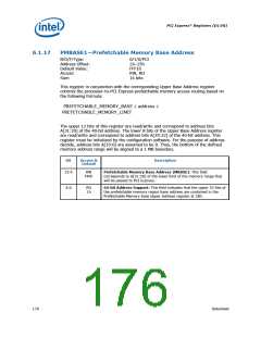
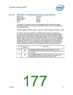
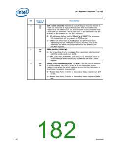
PCI Express* Registers (D1:F0)
6.1.19
PMBASEU1—Prefetchable Memory Base Address
B/D/F/Type:
Address Offset:
Default Value:
Access:
0/1/0/PCI
28–2Bh
00000000h
RW
Size:
32 bits
The functionality associated with this register is present in the PEG design
implementation.
This register in conjunction with the corresponding Upper Base Address register
controls the processor-to-PCI Express prefetchable memory access routing based on
the following formula:
PREFETCHABLE_MEMORY_BASE ≤ address ≤ PREFETCHABLE_MEMORY_LIMIT
The upper 12 bits of this register are read/write and correspond to address bits
A[31:20] of the 40-bit address. The lower 8 bits of the Upper Base Address register
are read/write and correspond to address bits A[39:32] of the 40-bit address. This
register must be initialized by the configuration software. For the purpose of address
decode, address bits A[19:0] are assumed to be 0. Thus, the bottom of the defined
memory address range will be aligned to a 1 MB boundary.
Bit
Description
Access &
Default
31:0
Prefetchable Memory Base Address (MBASEU): This field
corresponds to A[63:32] of the lower limit of the prefetchable
memory range that will be passed to PCI Express.
RW
00000000h
178
Datasheet

 INTEL [ INTEL ]