PCI Express* Registers (D1:F0)
Bit
Access &
Default
Description
2
ISA Enable (ISAEN): Needed to exclude legacy resource decode to
route ISA resources to legacy decode path. This bit modifies the
response by the GMCH to an I/O access issued by the processor that
target ISA I/O addresses. This applies only to I/O addresses that are
enabled by the IOBASE and IOLIMIT registers.
RW
0b
0 = All addresses defined by the IOBASE and IOLIMIT for processor
I/O transactions will be mapped to PCI Express.
1 = GMCH will not forward to PCI Express any I/O transactions
addressing the last 768 bytes in each 1 KB block even if the
addresses are within the range defined by the IOBASE and
IOLIMIT registers.
1
0
SERR Enable (SERREN):
RW
0b
0 = No forwarding of error messages from secondary side to primary
side that could result in an SERR.
1 = ERR_COR, ERR_NONFATAL, and ERR_FATAL messages result in
SERR message when individually enabled by the Root Control
register.
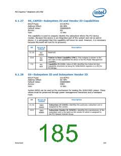
Parity Error Response Enable (PEREN): This bit controls whether
or not the Master Data Parity Error bit in the Secondary Status
register is set when the GMCH receives across the link (upstream) a
Read Data Completion Poisoned TLP.
RW
0b
0 = Master Data Parity Error bit in Secondary Status register can NOT
be set.
1 = Master Data Parity Error bit in Secondary Status register CAN be
set.
182
Datasheet

 INTEL [ INTEL ]