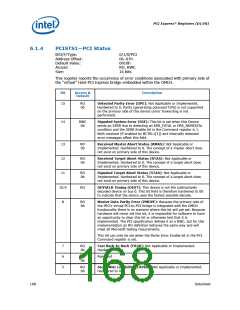
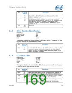
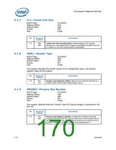
PCI Express* Registers (D1:F0)
6.1.12
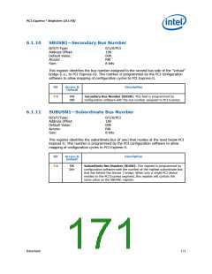
IOBASE1—I/O Base Address
B/D/F/Type:
Address Offset:
Default Value:
Access:
0/1/0/PCI
1Ch
F0h
RW, RO
8 bits
Size:
This register controls the processor to PCI Express-G I/O access routing based on the
following formula:
IO_BASE ≤ address ≤ IO_LIMIT
Only the upper 4 bits are programmable. For the purpose of address decode, address
bits A[11:0] are treated as 0. Thus the bottom of the defined I/O address range will
be aligned to a 4 KB boundary.
Bit
7:4
3:0
Access &
Default
Description
RW
Fh
I/O Address Base (IOBASE): This field corresponds to A[15:12] of
the I/O addresses passed by bridge 1 to PCI Express.
RO
0h
Reserved
6.1.13
IOLIMIT1—I/O Limit Address
B/D/F/Type:
Address Offset:
Default Value:
Access:
0/1/0/PCI
1Dh
00h
RW, RO
8 bits
Size:
This register controls the processor to PCI Express-G I/O access routing based on the
following formula:
IO_BASE ≤ address ≤ IO_LIMIT
Only the upper 4 bits are programmable. For the purpose of address decode, address
bits A[11:0] are assumed to be FFFh. Thus, the top of the defined I/O address range
will be at the top of a 4 KB aligned address block.
Bit
Access &
Default
Description
7:4
RW
0h
I/O Address Limit (IOLIMIT): This field corresponds to A[15:12] of
the I/O address limit of device 1. Devices between this upper limit and
IOBASE1 will be passed to the PCI Express hierarchy associated with
this device.
3:0
RO
0h
Reserved
172
Datasheet

 INTEL [ INTEL ]