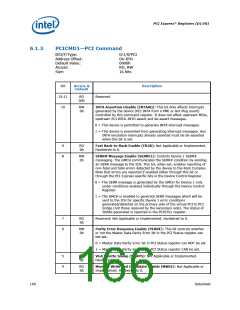
PCI Express* Registers (D1:F0)
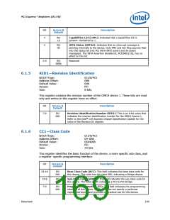
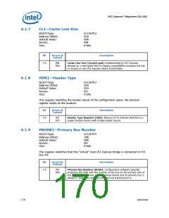
6.1.7
CL1—Cache Line Size
B/D/F/Type:
Address Offset:
Default Value:
Access:
0/1/0/PCI
0Ch
00h
RW
8 bits
Size:
Bit
Access &
Default
Description
7:0
RW
00h
Cache Line Size (Scratch pad): Implemented by PCI Express
devices as a read-write field for legacy compatibility purposes but has
no impact on any PCI Express device functionality.
6.1.8
HDR1—Header Type
B/D/F/Type:
Address Offset:
Default Value:
Access:
0/1/0/PCI
0Eh
01h
RO
8 bits
Size:
This register identifies the header layout of the configuration space. No physical
register exists at this location.
Bit
Access &
Default
Description
7:0
RO
Header Type Register (HDR): Returns 01 to indicate that this is a
01h
single function device with bridge header layout.
6.1.9
PBUSN1—Primary Bus Number
B/D/F/Type:
Address Offset:
Default Value:
Access:
0/1/0/PCI
18h
00h
RO
8 bits
Size:
This register identifies that this "virtual" Host-PCI Express bridge is connected to PCI
bus #0.
Bit
Access &
Default
Description
7:0
RO
00h
Primary Bus Number (BUSN): Configuration software typically
programs this field with the number of the bus on the primary side of
the bridge. Since device 1 is an internal device and its primary bus is
always 0, these bits are read only and are hardwired to 0.
170
Datasheet

 INTEL [ INTEL ]