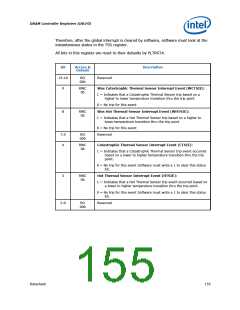
DRAM Controller Registers (D0:F0)
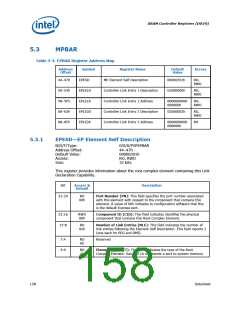
5.3
MPBAR
Table 5-4. EPBAR Register Address Map
Address
Offset
Symbol
Register Name
Default
Value
Access
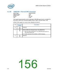
44–47h
50–53h
58–5Fh
60–63h
68–6Fh
EPESD
ME Element Self Description
00000201h
01000000h
RO,
RWO
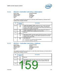
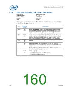
EPLE1D
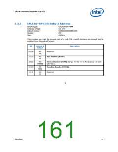
EPLE1A
EPLE2D
EPLE2A
Controller Link Entry 1 Description
Controller Link Entry 1 Address
Controller Link Entry 2 Description
Controller Link Entry 2 Address
RO,
RWO
0000000000
000000h
RO,
RWO
02000002h
RO,
RWO
0000000000
008000h
RO
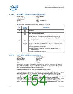
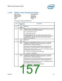
5.3.1
EPESD—EP Element Self Description
B/D/F/Type:
Address Offset:
Default Value:
Access:
0/0/0/PXPEPBAR
44–47h
00000201h
RO, RWO
Size:
32 bits
This register provides information about the root complex element containing this Link
Declaration Capability.
Bit
Access &
Default
Description
31:24
RO
00h
Port Number (PN): This field specifies the port number associated
with this element with respect to the component that contains this
element. A value of 00h indicates to configuration software that this
is the default Express port.
23:16
15:8
RWO
00h
Component ID (CID): This field indicates identifies the physical
component that contains this Root Complex Element.
RO
0sh
Number of Link Entries (NLE): This field indicates the number of
link entries following the Element Self Description. This field reports 2
(one each for PEG and DMI).
7:4
3:0
RO
0h
Reserved
RO
1h
Element Type (ET): This field indicates the type of the Root
Complex Element. Value of 1h represents a port to system memory.
158
Datasheet

 INTEL [ INTEL ]