DRAM Controller Registers (D0:F0)
5.2.49
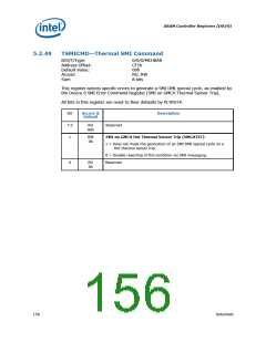
TSMICMD—Thermal SMI Command
B/D/F/Type:
Address Offset:
Default Value:
Access:
0/0/0/MCHBAR
CF1h
00h
RO, RW
8 bits
Size:
This register selects specific errors to generate a SMI DMI special cycle, as enabled by
the Device 0 SMI Error Command Register [SMI on GMCH Thermal Sensor Trip].
All bits in this register are reset to their defaults by PLTRST#.
Bit
7:2
1
Access &
Default
Description
RO
00h
Reserved
RW
0b
SMI on GMCH Hot Thermal Sensor Trip (SMGHTST):
1 = Does not mask the generation of an SMI DMI special cycle on a
Hot thermal sensor trip.
0 = Disable reporting of this condition via SMI messaging.
Reserved
0
RO
0b
156
Datasheet

 INTEL [ INTEL ]