DRAM Controller Registers (D0:F0)
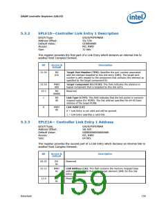
5.3.2
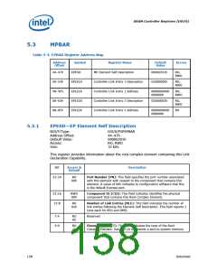
EPLE1D—Controller Link Entry 1 Description
B/D/F/Type:
Address Offset:
Default Value:
Access:
0/0/0/PXPEPBAR
50–53h
01000000h
RO, RWO
Size:
32 bits
This register provides the first part of a Link Entry which declares an internal link to
another Root Complex Element.
Bit
Access &
Default
Description
31:24
RO
01h
Target Port Number (TPN): Specifies the port number associated
with the element targeted by this link entry (DMI). The target port
number is with respect to the component that contains this element as
specified by the target component ID.
23:16
15:2
1
RWO
00h
Target Component ID (TCID): This field indicates the physical or
logical component that is targeted by this link entry.
RO
0000h
Reserved
RO
0b
Link Type (LTYP): This field indicates that the link points to memory-
mapped space (for RCRB). The link address specifies the 64-bit base
address of the target RCRB.
0
RWO
0b
Link Valid (LV):
0 = Link Entry is not valid and will be ignored.
1 = Link Entry specifies a valid link.
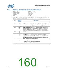
5.3.3
EPLE1A— Controller Link Entry 1 Address
B/D/F/Type:
Address Offset:
Default Value:
Access:
0/0/0/PXPEPBAR
58–5Fh
0000000000000000h
RO, RWO
Size:
64 bits
This register provides the second part of a Link Entry which declares an internal link to
another Root Complex Element.
Bit
Access &
Default
Description
63:32
31:12
RO
0s
Reserved
RWO
0s
Link Address (LA): This field contains the memory mapped base
address of the RCRB that is the target element (DMI) for this link
entry.
11:0
RO
0s
Reserved
Datasheet
159

 INTEL [ INTEL ]