DRAM Controller Registers (D0:F0)
5.2.46
TCO—Thermal Calibration Offset
B/D/F/Type:
Address Offset:
Default Value:
Access:
0/0/0/MCHBAR
CE2h
00h
RW/L/K, RW/L
8 bits
Size:
Bit 7 is reset to its default by PLTRST#. Bits 6:0 are reset to their defaults by
CL_PWROK.
Bit
Access &
Default
Description
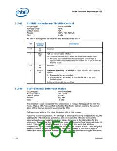
7
RW/L/K
0b
Lock Bit for Catastrophic (LBC): This bit, when written to a 1, locks
the Catastrophic programming interface, including bits 7:0 of this
register and bits 15:0 of TSTTP, bits 1,7 of TSC 1, bits 3:0 of TSC 2,
bits 4:0 of TSC 3, and bits 0,7 of TST. This bit may only be set to a 0
by a hardware reset (PLTRST#). Writing a 0 to this bit has no effect.
6:0
RW/L
00h
Calibration Offset (CO): This field contains the current calibration
offset for the Thermal Sensor DAC inputs. The calibration offset is a
twos complement signed number which is added to the temperature
counter value to help generate the final value going to the thermal
sensor DAC. This register is loaded by the hardware from fuses that
are blown during test.
This field is Read/Write, but should be kept at its default value as
programmed by the fuses in the part.
Note for TCO operation:
While this is a seven-bit field, the 7th bit is sign extended to 9 bits for
TCO operation. The range of 00h to 3Fh corresponds to 0 0000 0000
to 0 0011 1111. The range of 41h to 7fh corresponds to 1 1100 001
(i.e., negative 3fh) to 1 1111 1111 (i.e., negative 1), respectively.
Datasheet
153

 INTEL [ INTEL ]