DRAM Controller Registers (D0:F0)
5.2.44
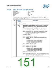
TSS—Thermal Sensor Status
B/D/F/Type:
Address Offset:
Default Value:
Access:
0/0/0/MCHBAR
CDAh
00h
RO
8 bits
Size:
This read only register provides trip point and other status of the thermal sensor. All
bits in this register are reset to their defaults by CL_PWROK.
Bit
Access &
Default
Description
7
RO
0b
Catastrophic Trip Indicator (CTI):
1 = Internal thermal sensor temperature is above the catastrophic
setting.
6
RO
0b
Hot Trip Indicator (HTI):
1 = Internal thermal sensor temperature is above the Hot setting.
Reserved
5:0
RO
0s
5.2.45
TSTTP—Thermal Sensor Temperature Trip Point
B/D/F/Type:
Address Offset:
Default Value:
Access:
0/0/0/MCHBAR
CDC–CDFh
00000000h
RO, RW, RW/L
32 bits
Size:
This register sets the target values for the trip points.
All bits in this register are reset to their defaults by CL_PWROK.
Bit
Access &
Default
Description
31:16
15:8
RO
0000h
Reserved
RW/L
00h
Hot Trip Point Setting (HTPS): Sets the target value for the Hot
trip point.
Lockable via TCO bit 7.
7:0
RW/L
00h
Catastrophic Trip Point Setting (CTPS): Sets the target for the
Catastrophic trip point. See also TST[Direct DAC Connect Test
Enable].
Lockable via TCO bit 7.
152
Datasheet

 INTEL [ INTEL ]