DRAM Controller Registers (D0:F0)
5.2.43
TSC2—Thermal Sensor Control 2
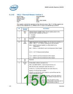
B/D/F/Type:
Address Offset:
Default Value:
Access:
0/0/0/MCHBAR
CD9h
00h
RW/L, RO
8 bits
Size:
This register controls the operation of the thermal sensor. All bits in this register are
reset to their defaults by CL_PWROK.
Bit
7:4
3:0
Access &
Default
Description
RO
0h
Reserved
RW/L
0h
Thermometer Mode Enable and Rate (TE): These bits enable the
thermometer mode functions and set the Thermometer controller
rate.
The trip points (Catastrophic and Hot) will all operate using the
programmed trip points and Thermometer mode rate.
Note: During boot, all other thermometer mode registers (except
lock bits) should be programmed appropriately before
enabling the Thermometer Mode.
Lockable via TCO bit 7.
0000 = Thermometer mode disabled
0100 = enabled, 2048 clock mode (normal Thermometer mode
operation)
- provides ~7.68uS settling time @ 266MHz
- provides ~6.14us settling time @ 333MHz
- provides ~5.12us settling time @ 400MHz
0101 = enabled, 3072 clock mode
0110 = enabled, 4096 clock mode
0111 = enabled, 6144 clock mode
- provides ~23.1uS settling time @ 266MHz
- provides ~18.5us settling time @ 333MHz
- provides ~15.4uS settling time @ 400MHz
all other bit encodings are reserved
NOTE: The settling time for DAC and Thermal Diode is between 2 and
5 micro-seconds. To meet this requirement the SE value must
be programmed to be 5 micro-seconds or more.
Recommendation is to use 0100 setting.
Datasheet
151

 INTEL [ INTEL ]