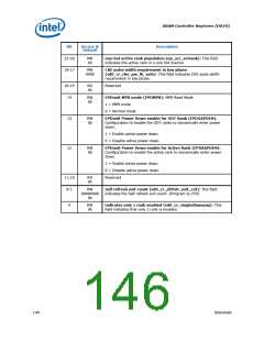
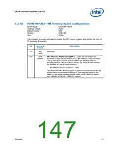
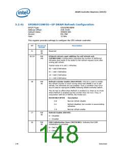
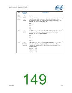
DRAM Controller Registers (D0:F0)
5.2.42
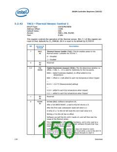
TSC1—Thermal Sensor Control 1
B/D/F/Type:
Address Offset:
Default Value:
Access:
0/0/0/MCHBAR
CD8h
00h
RW/L, RW, RS/WC
8 bits
Size:
This register controls the operation of the thermal sensor. Bits 7:1 of this register are
reset to their defaults by CL_PWROK. Bit 0 is reset to its default by PLTRST#.
Bit
Access &
Default
Description
7
RW/L
0b
Thermal Sensor Enable (TSE): This bit enables power to the
thermal sensor. Lockable via TCO bit 7.
0 = Disabled
1 = Enabled
Reserved
6
RO
0b
5:2
RW
Digital Hysteresis Amount (DHA): This bit determines whether no
0000b
offset, 1 LSB, 2... 15 is used for hysteresis for the trip points.
0000 = digital hysteresis disabled, no offset added to trip
temperature
0001 = offset is 1 LSB added to each trip temperature when tripped
...
0110 = ~3.0 °C (Recommended setting)
...
1110 = added to each trip temperature when tripped
1111 = added to each trip temperature when tripped
Reserved
1
0
RO
0b
RS/WC
0b
In Use (IU): Software semaphore bit.
After a full GMCH RESET, a read to this bit returns a 0.
After the first read, subsequent reads will return a 1.
A write of a 1 to this bit will reset the next read value to 0.
Writing a 0 to this bit has no effect.
Software can poll this bit until it reads a 0, and will then own the
usage of the thermal sensor.
This bit has no other effect on the hardware, and is only used as a
semaphore among various independent software threads that may
need to use the thermal sensor.
Software that reads this register but does not intend to claim
exclusive access of the thermal sensor must write a one to this bit if it
reads a 0, in order to allow other software threads to claim it.
150
Datasheet

 INTEL [ INTEL ]