DRAM Controller Registers (D0:F0)
5.2.40
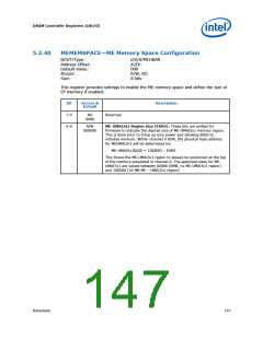
MEMEMSPACE—ME Memory Space Configuration
B/D/F/Type:
Address Offset:
Default Value:
Access:
0/0/0/MCHBAR
A2Eh
00h
R/W, RO
8 bits
Size:
This register provides settings to enable the ME memory space and define the size of
EP memory if enabled.
Bit
7:5
4:0
Access &
Default
Description
RO
000b
Reserved
R/W
00000b
ME-UMA(Sx) Region Size (EXRS): These bits are written by
firmware to indicate the desired size of ME-UMA(Sx) memory region.
This is done prior to bring up core power and allowing BIOS to
initialize memory. Within channel 0 DDR, the physical base address
for MEUMA(Sx) will be determined by:
ME-UMA(Sx)BASE = C0DRB3 – EXRS
This forces the ME-UMA(Sx) region to always be positioned at the top
of the memory populated in channel 0. The approved sizes for ME-
UMA(Sx) are values between 0000b (0MB, no ME-UMA(Sx) region)
and 10000b (16 MB ME – UMA(Sx) region)
Datasheet
147

 INTEL [ INTEL ]