DRAM Controller Registers (D0:F0)
Bit
Access &
Default
Description
13:9
RW
00000b
Same Rank READ to WRITE Delayed (C0sd_cr_wrsr_rd): This
field indicates the minimum allowed spacing (in DRAM clocks) between
the READ and WRITE commands.
8:6
5:3
RO
0h
Reserved
RW
000b
Same Rank Read To Read Delayed (C0sd_cr_rdsr_rd): This field
indicates the minimum allowed spacing (in DRAM clocks) between two
READ commands to the same rank.
2:0
RO
0h
Reserved
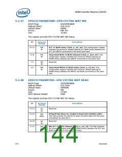
5.2.39
EPDCKECONFIGREG—EPD CKE Related Configuration
Register
B/D/F/Type:
Address Offset:
Default Value:
Access:
0/0/0/MCHBAR
A28–A2Ch
00E0000000h
RW
Size:
40 bits
BIOS Optimal Default
0h
This register provides CKE related configuration for EPD.
Bit
Access &
Default
Description
39:35
RW
00000b
EPDunit TXPDLL Count (EPDTXPDLL): This field specifies the delay
from precharge power down exit to a command that requires the
DRAM DLL to be operational. The commands are read/write.
34:32
31:29
RW
000b
EPDunit TXP count (EPDCKETXP): This field specifies the timing
requirement for Active power down exit or fast exit pre-charge power
down exit to any command or slow exit pre-charge power down to
Non-DLL (rd/wr/odt) command.
RW
Mode Select (sd0_cr_sms): This field indicates the mode in which
111b
the controller is operating in.
111 = indicates normal mode of operation, else special mode of
operation.
28:27
26:24
RW
00b
EPDunit EMRS command select. (EPDEMRSSEL): EMRS mode to
select BANK address.
01 = EMRS
10 = EMRS2
11 = EMRS3
RW
000b
CKE pulse width requirement in high phase
(sd0_cr_cke_pw_hl_safe): This field indicates CKE pulse width
requirement in high phase.
Datasheet
145

 INTEL [ INTEL ]