DRAM Controller Registers (D0:F0)
5.2.37
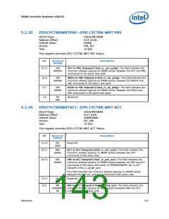
EPDCYCTRKWRTWR—EPD CYCTRK WRT WR
B/D/F/Type:
Address Offset:
Default Value:
Access:
0/0/0/MCHBAR
A20–A21h
0000h
RW, RO
16 bits
Size:
This register provides EPD CYCTRK WRT WR Status.
Bit
Access &
Default
Description
15:12
RW
0h
ACT To Write Delay (C0sd_cr_act_wr): This configuration register
indicates the minimum allowed spacing (in DRAM clocks) between the
ACT and WRITE commands to the same rank-bank.
11:8
RW
0h
Same Rank Write To Write Delayed (C0sd_cr_wrsr_wr): This
configuration register indicates the minimum allowed spacing (in
DRAM clocks) between two WRITE commands to the same rank.
7:4
3:0
RO
0h
Reserved
RW
0h
Same Rank WRITE to READ Delay (C0sd_cr_rd_wr): This
configuration register indicates the minimum allowed spacing (in
DRAM clocks) between the WRITE and READ commands to the same
rank
5.2.38
EPDCYCTRKWRTRD—EPD CYCTRK WRT READ
B/D/F/Type:
Address Offset:
Default Value:
Access:
0/0/0/MCHBAR
A24–A26h
000000h
RW
Size:
24 bits
BIOS Optimal Default
000h
This register provides EPD CYCTRK WRT RD Status.
Bit
Access &
Default
Description
23:23
22:20
Reserved
RO
0h
EPDunit DQS Slave DLL Enable to Read Safe (EPDSDLL2RD):
This field provides the setting for Read command safe from the point
of enabling the slave DLLs.
RW
000b
19:18
17:14
Reserved
RO
0h
Min ACT To READ Delayed (C0sd_cr_act_rd): This field indicates
the minimum allowed spacing (in DRAM clocks) between the ACT and
READ commands to the same rank-bank.
RW
0h
144
Datasheet

 INTEL [ INTEL ]