DRAM Controller Registers (D0:F0)
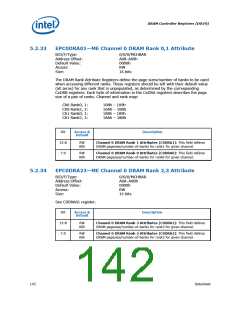
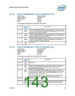
5.2.35
EPDCYCTRKWRTPRE—EPD CYCTRK WRT PRE
B/D/F/Type:
Address Offset:
Default Value:
Access:
0/0/0/MCHBAR
A19–A1Ah
0000h
RW, RO
16 bits
Size:
This register provides EPD CYCTRK WRT PRE Status.
Bit
Access &
Default
Description
15:11
RW
00000b
ACT to PRE Delayed (C0sd_cr_act_pchg): This field indicates the
minimum allowed spacing (in DRAM clocks) between the ACT and PRE
commands to the same rank-bank
10:6
5:2
RW
00000b
Write to PRE Delayed (C0sd_cr_wr_pchg): This field indicates the
minimum allowed spacing (in DRAM clocks) between the WRITE and
PRE commands to the same rank-bank
RW
0000b
READ to PRE Delayed (C0sd_cr_rd_pchg): This field indicates the
minimum allowed spacing (in DRAM clocks) between the READ and
PRE commands to the same rank-bank
1:0
RO
Reserved
00b
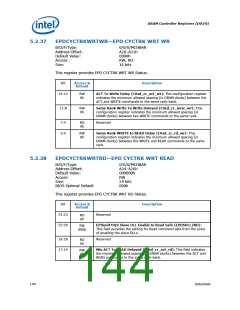
5.2.36
EPDCYCTRKWRTACT—EPD CYCTRK WRT ACT
B/D/F/Type:
Address Offset:
Default Value:
Access:
0/0/0/MCHBAR
A1C–A1Fh
00000000h
RO, RW
Size:
32 bits
This register provides EPD CYCTRK WRT ACT Status.
Bit
Access &
Default
Description
31:21
20:17
RO
000h
Reserved
RW
0000b
ACT to ACT Delayed (C0sd_cr_act_act[): This field indicates the
minimum allowed spacing (in DRAM clocks) between two ACT
commands to the same rank.
16:13
RW
0000b
PRE to ACT Delayed (C0sd_cr_pre_act): This field indicates the
minimum allowed spacing (in DRAM clocks) between the PRE and ACT
commands to the same rank-bank:12:9R/W0000bPRE-ALL to ACT
Delayed (C0sd_cr_preall_act):
This field indicates the minimum allowed spacing (in DRAM clocks)
between the PRE-ALL and ACT commands to the same rank.
12:9
8:0
RO
0h
Reserved
RW
00000000
0b
REF to ACT Delayed (C0sd_cr_rfsh_act): This field indicates the
minimum allowed spacing (in DRAM clocks) between REF and ACT
commands to the same rank.
Datasheet
143

 INTEL [ INTEL ]