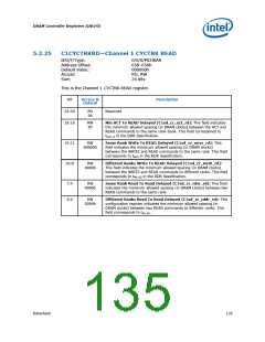
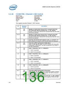
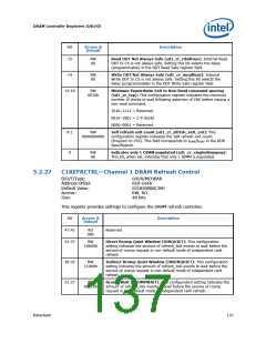
DRAM Controller Registers (D0:F0)
Bit
Access &
Default
Description
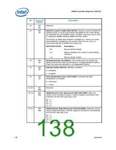
15:14
RW
00b
DRAM Refresh Low Watermark (REFLOWWM): When the refresh
count exceeds this level, a refresh request is launched to the scheduler
and the dref_low flag is set.
00 = 1
01 = 2
10 = 3
11 = 4
13:0
RW
00110000
110000b
Refresh Counter Time Out Value (REFTIMEOUT): Program this
field with a value that will provide 7.8 us at the memory clock
frequency. At various memory clock frequencies this results in the
following values:
266 MHz -> 820h
333 MHz -> A28h
400 MHz -> C30h
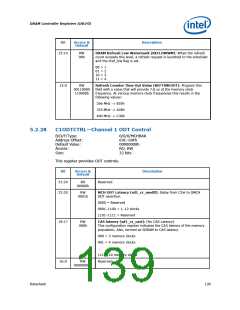
5.2.28
C1ODTCTRL—Channel 1 ODT Control
B/D/F/Type:
Address Offset:
Default Value:
Access:
0/0/0/MCHBAR
69C–69Fh
00000000h
RO, RW
Size:
32 bits
This register provides ODT controls.
Bit
Access &
Default
Description
31:24
23:20
RO
00000h
Reserved
RW
MCH ODT Latency (sd1_cr_modtl): Delay from CS# to GMCH
0001b
ODT assertion.
0000 = Reserved
0001–1100 = 1–12 clocks
1101–1111 = Reserved
19:17
RW
CAS latency (sd1_cr_casl): (for CAS Latency)
000b
This configuration register indicates the CAS latency of the memory
population. Also, termed as SDRAM to CAS latency.
000 = 3 memory clocks
001 = 4 memory clocks
…
111 = 10 memory clocks
Reserved
16:0
RW
00000000h
Datasheet
139

 INTEL [ INTEL ]