DRAM Controller Registers (D0:F0)
5.2.9
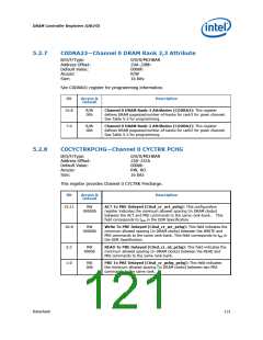
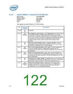
C0CYCTRKACT—Channel 0 CYCTRK ACT
B/D/F/Type:
Address Offset:
Default Value:
Access:
0/0/0/MCHBAR
252–255h
00000000h
RW, RO
Size:
32 bits
This register provides Channel 0 CYCTRK Activate.
Bit
Access &
Default
Description
31:28
27:22
RO
0h
Reserved
RW
000000b
ACT Window Count (C0sd_cr_act_windowcnt): This field indicates
the window duration (in DRAM clocks) during which the controller
counts the # of activate commands which are launched to a particular
rank. If the number of activate commands launched within this window
is greater than 4, then a check is implemented to block launch of
further activates to this rank for the rest of the duration of this
window.
21
RW
0b
Max ACT Check Disable (C0sd_cr_maxact_dischk): This field
disenables the check which ensures that there are no more than four
activates to a particular rank in a given window.
20:17
RW
0000b
ACT to ACT Delayed (C0sd_cr_act_act[): This field indicates the
minimum allowed spacing (in DRAM clocks) between two ACT
commands to the same rank. This field corresponds to tRRD in the DDR
Specification.
16:13
RW
0000b
PRE to ACT Delayed (C0sd_cr_pre_act): This field indicates the
minimum allowed spacing (in DRAM clocks) between the PRE and ACT
commands to the same rank-bank. This field corresponds to tRP in the
DDR Specification.
12:9
8:0
RW
0h
ALLPRE to ACT Delay (C0sd0_cr_preall_act): From the launch of a
prechargeall command wait for these many # of memory clocks before
launching a activate command. This field corresponds to tPALL_RP
.
RW
00000000
0b
REF to ACT Delayed (C0sd_cr_rfsh_act): This configuration
register indicates the minimum allowed spacing (in DRAM clocks)
between REF and ACT commands to the same rank. This field
corresponds to tRFC in the DDR Specification.
122
Datasheet

 INTEL [ INTEL ]