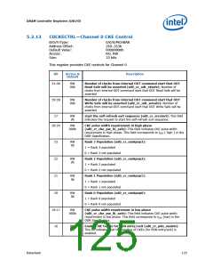
DRAM Controller Registers (D0:F0)
5.2.7
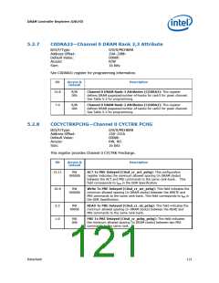
C0DRA23—Channel 0 DRAM Rank 2,3 Attribute
B/D/F/Type:
Address Offset:
Default Value:
Access:
0/0/0/MCHBAR
20A–20Bh
0000h
R/W
16 bits
Size:
See C0DRA01 register for programming information.
Bit
Access &
Default
Description
15:8
R/W
00h
Channel 0 DRAM Rank-3 Attributes (CODRA3): This register
defines DRAM pagesize/number-of-banks for rank3 for given channel.
See Table 5-3 for programming.
7:0
R/W
00h
Channel 0 DRAM Rank-2 Attributes (CODRA2): This register
defines DRAM pagesize/number-of-banks for rank2 for given channel.
See Table 5-3 for programming.
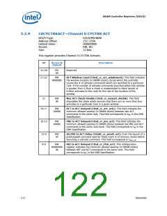
5.2.8
C0CYCTRKPCHG—Channel 0 CYCTRK PCHG
B/D/F/Type:
Address Offset:
Default Value:
Access:
0/0/0/MCHBAR
250–251h
0000h
RW, RO
16 bits
Size:
This register provides Channel 0 CYCTRK Precharge.
Bit
Access &
Default
Description
15:11
RW
00000b
ACT To PRE Delayed (C0sd_cr_act_pchg): This configuration
register indicates the minimum allowed spacing (in DRAM clocks)
between the ACT and PRE commands to the same rank-bank. This
field corresponds to tRAS in the DDR Specification.
10:6
RW
00000b
Write To PRE Delayed (C0sd_cr_wr_pchg): This field indicates the
minimum allowed spacing (in DRAM clocks) between the WRITE and
PRE commands to the same rank-bank. This field corresponds to tWR in
the DDR Specification.
5:2
1:0
RW
0000b
READ To PRE Delayed (C0sd_cr_rd_pchg): This field indicates the
minimum allowed spacing (in DRAM clocks) between the READ and
PRE commands to the same rank-bank.
RW
00b
PRE To PRE Delayed (C0sd_cr_pchg_pchg): This field indicates
the minimum allowed spacing (in DRAM clocks) between two PRE
commands to the same rank.
Datasheet
121

 INTEL [ INTEL ]