DRAM Controller Registers (D0:F0)
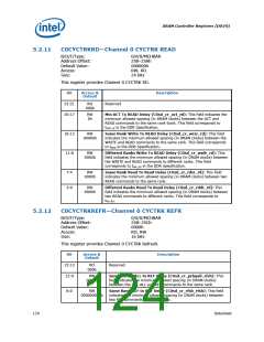
5.2.13
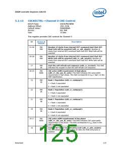
C0CKECTRL—Channel 0 CKE Control
B/D/F/Type:
Address Offset:
Default Value:
Access:
0/0/0/MCHBAR
260–263h
00000800h
RO, RW
Size:
32 bits
This register provides CKE controls for Channel 0
Bit
Access &
Default
Description
31:30
RW
00b
Number of clocks from internal ODT command start that ODT
Read Safe will be asserted (sd0_cr_odt_rdsafe): Number of
clocks from internal ODT command start that ODT Read Safe will be
asserted
29:28
RW
00b
Number of clocks from internal ODT command start that ODT
Write Safe will be asserted (sd0_cr_odt_wrsafe): Number of
clocks from internal ODT command start that ODT Write Safe will be
asserted
27
RW
0b
start the self-refresh exit sequence (sd0_cr_srcstart): This field
indicates the request to start the self-refresh exit sequence.
26:24
RW
000b
CKE pulse width requirement in high phase
(sd0_cr_cke_pw_hl_safe): This field indicates CKE pulse width
requirement in high phase. This field corresponds to tCKE ( high ) in the
DDR Specification.
23
22
21
20
RW
0b
Rank 3 Population (sd0_cr_rankpop3):
1 = Rank 3 populated
0 = Rank 3 not populated
RW
0b
Rank 2 Population (sd0_cr_rankpop2):
1 = Rank 2 populated
0 = Rank 2 not populated
RW
0b
Rank 1 Population (sd0_cr_rankpop1):
1 = Rank 1 populated
0 = Rank 1 not populated
RW
0b
Rank 0 Population (sd0_cr_rankpop0):
1 = Rank 0 populated
0 = Rank 0 not populated
19:17
16
RW
000b
CKE pulse width requirement in low phase
(sd0_cr_cke_pw_lh_safe): This field indicates CKE pulse width
requirement in low phase. This field corresponds to tCKE (low) in the
DDR Specification.
RW
0b
Enable CKE toggle for PDN entry/exit (sd0_cr_pdn_enable):
This bit indicates that the toggling of CKEs (for PDN entry/exit) is
enabled.
Datasheet
125

 INTEL [ INTEL ]