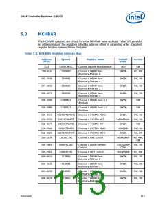
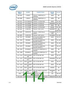
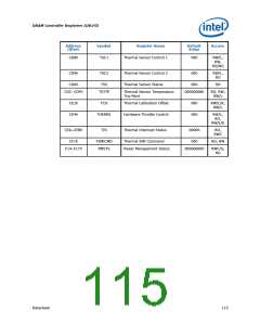
DRAM Controller Registers (D0:F0)
5.2.2
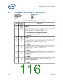
C0DRB0—Channel 0 DRAM Rank Boundary Address 0
B/D/F/Type:
Address Offset:
Default Value:
Access:
0/0/0/MCHBAR
200–201h
0000h
R/W, RO
16 bits
Size:
The DRAM Rank Boundary Registers define the upper boundary address of each DRAM
rank with a granularity of 64 MB. Each rank has its own single-word DRB register.
These registers are used to determine which chip select will be active for a given
address. Channel and rank map:
Ch 0, Rank 0 = 200h
Ch 0, Rank 1 = 202h
Ch 0, Rank 2 = 204h
Ch 0, Rank 3 = 206h
Ch 1, Rank 0 = 600h
Ch 1, Rank 1 = 602h
Ch 1, Rank 2 = 604h
Ch 1, Rank 3 = 606h
Programming Guide
If Channel 0 is empty, all of the C0DRBs are programmed with 00h.
C0DRB0 = Total memory in Ch 0, Rank 0 (in 64 MB increments)
C0DRB1 = Total memory in Ch 0, Rank 0 + Ch 0, Rank 1 (in 64 MB increments)
…
If Channel 1 is empty, all of the C1DRBs are programmed with 00h
C1DRB0= Total memory in Ch 1, Rank 0 (in 64 MB increments)
C1DRB1= Total memory in Ch 1, Rank 0 + Ch 1, Rank 1 (in 64 MB increments)
...
For Flex Memory Mode
C1DRB0, C1DRB1, and C1DRB2:
They are also programmed similar to non-Flex mode. Only exception is, the DRBs
corresponding to the top most populated rank and higher ranks in Channel 1 must be
programmed with the value of the total Channel 1 population plus the value of total
Channel 0 population (C0DRB3).
Example: If only Ranks 0 and 1 are populated in Ch1 in Flex mode, then:
C1DRB0 = Total memory in Ch 1, Rank 0 (in 64MB increments)
C1DRB1 = C0DRB3 + Total memory in Ch 1, Rank 0 + Ch 1, Rank 1 (in 64 MB
increments) (Rank 1 is the topmost populated rank)
C1DRB2 = C1DRB1
C1DRB3 = C1DRB1
C1DRB3:
C1DRB3 = C0DRB3 + Total memory in Channel 1.
Datasheet
117

 INTEL [ INTEL ]