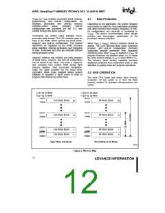
INTEL StrataFlash™ MEMORY TECHNOLOGY, 32 AND 64 MBIT
E
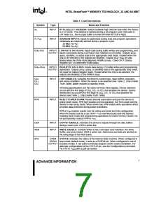
Table 1. Lead Descriptions (Continued)
Symbol
BYTE#
Type
Name and Function
INPUT BYTE ENABLE: BYTE# low places the device in x8 mode. All data is then input
or output on DQ0–DQ7, while DQ8–DQ15 float. Address A0 selects between the
high and low byte. BYTE# high places the device in x16 mode, and turns off the
A0 input buffer. Address A1 then becomes the lowest order address.
VPEN
INPUT ERASE / PROGRAM / BLOCK LOCK ENABLE: For erasing array blocks,
programming data, or configuring lock-bits.
With VPEN ≤ VPENLK, memory contents cannot be altered.
VCC
SUPPLY DEVICE POWER SUPPLY: With VCC ≤ VLKO, all write attempts to the flash
memory are inhibited.
VCCQ
OUTPUT OUTPUT BUFFER POWER SUPPLY: This voltage controls the device’s output
BUFFER voltages. To obtain output voltages compatible with system data bus voltages,
SUPPLY connect VCCQ to the system supply voltage.
GND
NC
SUPPLY GROUND: Do not float any ground pins.
NO CONNECT: Lead is not internally connected; it may be driven or floated.
8
ADVANCE INFORMATION

 INTEL [ INTEL ]