E
INTEL StrataFlash™ MEMORY TECHNOLOGY, 32 AND 64 MBIT
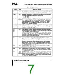
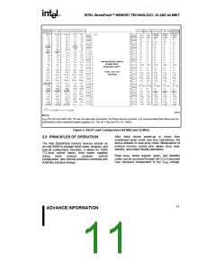
Table 1. Lead Descriptions
Name and Function
Symbol
Type
A0
INPUT BYTE-SELECT ADDRESS: Selects between high and low byte when the device
is in x8 mode. This address is latched during a x8 program cycle. Not used in
x16 mode (i.e., the A0 input buffer is turned off when BYTE# is high).
A1–A22
INPUT ADDRESS INPUTS: Inputs for addresses during read and program operations.
Addresses are internally latched during a program cycle.
32-Mbit: A0–A21
64-Mbit: A0–A22
DQ0–DQ7
INPUT/ LOW-BYTE DATA BUS: Inputs data during buffer writes and programming, and
OUTPUT inputs commands during Command User Interface (CUI) writes. Outputs array,
query, identifier, or status data in the appropriate read mode. Floated when the
chip is de-selected or the outputs are disabled. Outputs DQ6–DQ0 are also
floated when the Write State Machine (WSM) is busy. Check SR.7 (Status
Register bit 7) to determine WSM status.
DQ8–DQ15
INPUT/ HIGH-BYTE DATA BUS: Inputs data during x16 buffer writes and programming
OUTPUT operations. Outputs array, query, or identifier data in the appropriate read mode;
not used for Status Register reads. Floated when the chip is de-selected, the
outputs are disabled, or the WSM is busy.
CE0,
CE1,
CE2
INPUT CHIP ENABLES: Activates the device’s control logic, input buffers, decoders,
and sense amplifiers. When the device is de-selected (see Table 2, Chip Enable
Truth Table), power reduces to standby levels.
All timing specifications are the same for these three signals. Device selection
occurs with the first edge of CE0, CE1, or CE2 that enables the device. Device
deselection occurs with the first edge of CE0, CE1, or CE2 that disables the
device (see Table 2, Chip Enable Truth Table).
RP#
INPUT RESET/ POWER-DOWN: Resets internal automation and puts the device in
power-down mode. RP#-high enables normal operation. Exit from reset sets the
device to read array mode. When driven low, RP# inhibits write operations which
provides data protection during power transitions.
RP# at VHH enables master lock-bit setting and block lock-bits configuration
when the master lock-bit is set. RP# = VHH overrides block lock-bits thereby
enabling block erase and programming operations to locked memory blocks. Do
not permanently connect RP# to VHH
.
OE#
WE#
INPUT OUTPUT ENABLE: Activates the device’s outputs through the data buffers
during a read cycle. OE# is active low.
INPUT WRITE ENABLE: Controls writes to the Command User Interface, the Write
Buffer, and array blocks. WE# is active low. Addresses and data are latched on
the rising edge of the WE# pulse.
STS
OPEN
STATUS: Indicates the status of the internal state machine. When configured in
DRAIN level mode (default mode), it acts as a RY/BY# pin. When configured in one of
OUTPUT its pulse modes, it can pulse to indicate program and/or erase completion. For
alternate configurations of the STATUS pin, see the Configurations command.
Tie STS to VCCQ with a pull-up resistor.
7
ADVANCE INFORMATION

 INTEL [ INTEL ]