INTEL StrataFlash™ MEMORY TECHNOLOGY, 32 AND 64 MBIT
E
VPENH on VPEN enables successful block erasure,
programming, and lock-bit configuration. All
functions associated with altering memory
2.1
Data Protection
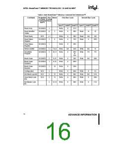
Depending on the application, the system designer
may choose to make the VPEN switchable (available
only when memory block erases, programs, or lock-
bit configurations are required) or hardwired to
contents—block
erase,
program,
lock-bit
configuration—are accessed via the CUI and
verified through the status register.
V
PENH. The device accommodates either design
Commands are written using standard micro-
processor write timings. The CUI contents serve as
input to the WSM, which controls the block erase,
program, and lock-bit configuration. The internal
algorithms are regulated by the WSM, including
pulse repetition, internal verification, and margining
of data. Addresses and data are internally latched
during program cycles.
practice and encourages optimization of the
processor-memory interface.
When VPEN ≤ VPENLK, memory contents cannot be
altered. The CUI’s two-step block erase, byte/word
program, and lock-bit configuration command
sequences provide protection from unwanted
operations even when VPENH is applied to VPEN. All
program functions are disabled when VCC is below
the write lockout voltage VLKO or when RP# is VIL.
The device’s block locking capability provides
additional protection from inadvertent code or data
alteration by gating erase and program operations.
Interface software that initiates and polls progress
of block erase, program, and lock-bit configuration
can be stored in any block. This code is copied to
and executed from system RAM during flash
memory updates. After successful completion,
reads are again possible via the Read Array
command. Block erase suspend allows system
software to suspend a block erase to read or
program data from/to any other block.
3.0 BUS OPERATION
The local CPU reads and writes flash memory
in-system. All bus cycles to or from the flash
memory conform to standard microprocessor bus
cycles.
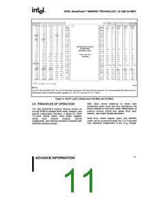
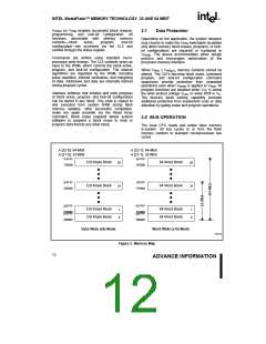
A [22-0]: 64-Mbit
A [21-0]: 32-Mbit
7FFFFF
A [22-1]: 64-Mbit
A [21-1]: 32-Mbit
3FFFFF
128-Kbyte Block
128-Kbyte Block
64-Word Block
64-Word Block
63
31
63
31
7E0000
3F0000
3FFFFF
3E0000
1FFFFF
1F0000
03FFFF
01FFFF
128-Kbyte Block
128-Kbyte Block
64-Word Block
64-Word Block
1
0
1
0
020000
01FFFF
010000
00FFFF
000000
000000
Byte-Wide (x8) Mode
Word Wide (x16) Mode
0606_05
Figure 5. Memory Map
12
ADVANCE INFORMATION

 INTEL [ INTEL ]