E
INTEL StrataFlash™ MEMORY TECHNOLOGY, 32 AND 64 MBIT
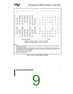
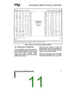
0606_04
NOTE:
VCC (Pin 42) and GND (Pin 15) are not internally connected. For future device revisions, it is recommended that these pins be
connected to their respected power supplies (i.e., Pin 42 = VCC and Pin 15 = GND).
Figure 4. SSOP Lead Configuration (64 Mbit and 32 Mbit)
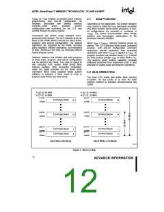
After initial device power-up or return from
reset/power-down mode (see Bus Operations), the
2.0 PRINCIPLES OF OPERATION
device defaults to read array mode. Manipulation of
external memory control pins allows array read,
standby, and output disable operations.
The Intel StrataFlash memory devices include an
on-chip WSM to manage block erase, program, and
lock-bit configuration functions. It allows for 100%
TTL-level control inputs, fixed power supplies
Read array, status register, query, and identifier
codes can be accessed through the CUI (Command
User Interface) independent of the VPEN voltage.
during
block
erasure,
program,
lock-bit
configuration, and minimal processor overhead with
RAM-like interface timings.
11
ADVANCE INFORMATION

 INTEL [ INTEL ]