INTEL StrataFlash™ MEMORY TECHNOLOGY, 32 AND 64 MBIT
E
FIGURES
TABLES
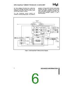
Figure 1. Intel StrataFlash™ Memory Block
Table 1. Lead Descriptions.................................7
Table 2. Chip Enable Truth Table.....................13
Table 3. Bus Operations...................................15
Diagram..............................................6
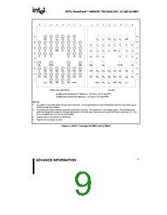
Figure 2. µBGA* Package (64-Mbit and 32-Mbit)9
Figure 3. TSOP Lead Configuration (32-Mbit)..10
Table 4. Intel StrataFlash™ Memory Command
Set Definitions ...................................16
Figure 4. SSOP Lead Configuration (64-Mbit
and 32-Mbit) .....................................11
Table 5. Summary of Query Structure Output as
a Function of Device and Mode .........19
Figure 5. Memory Map.....................................12
Figure 6. Device Identifier Code Memory Map .14
Figure 7. Write to Buffer Flowchart...................34
Figure 8. Byte/Word Program Flowchart ..........35
Figure 9. Block Erase Flowchart ......................36
Table 6. Example of Query Structure Output of
a x16- and x8-Capable Device...........19
Table 7. Query Structure..................................20
Table 8. Block Status Register .........................21
Table 9. CFI Identification ................................22
Table 10. System Interface Information............23
Table 11. Device Geometry Definition..............24
Figure 10. Block Erase Suspend/Resume
Flowchart..........................................37
Figure 11. Set Block Lock-Bit Flowchart...........38
Figure 12. Clear Block Lock-Bit Flowchart........39
Table 12. Primary Vendor-Specific Extended
Query.................................................25
Figure 13. Transient Input/Output Reference
Waveform for VCCQ = 5.0 V ± 10%
Table 13. Identifier Codes ................................26
Table 14. Write Protection Alternatives ............30
Table 15. Configuration Coding Definitions.......31
Table 16. Status Register Definitions ...............32
Table 17. eXtended Status Register Definitions33
(Standard Testing Configuration)......45
Figure 14. Transient Input/Output Reference
Waveform for VCCQ = 2.7 V−3.6V.....45
Figure 15. Transient Equivalent Testing Load
Circuit...............................................45
Figure 16. AC Waveform for Read Operations.47
Figure 17. AC Waveform for Write Operations .49
Figure 18. AC Waveform for Reset Operation..50
REVISION HISTORY
Date of
Revision
Version
Description
09/01/97
09/17/97
12/01/97
-001
-002
-003
Original Version
Modifications made to cover sheet
VCC/GND Pins Converted to No Connects specification change added
I
CCS, ICCD, ICCW, and ICCE specification change added
Order Codes specification change added
1/31/98
-004
The µBGA* chip-scale package in Figure 2 was changed to a 52-ball
package and appropriate documentation added. The 64-Mb µBGA
package dimensions were changed in Figure 2. Changed Figure 4 to
read SSOP instead of TSOP.
4
ADVANCE INFORMATION

 INTEL [ INTEL ]