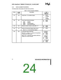
INTEL StrataFlash™ MEMORY TECHNOLOGY, 32 AND 64 MBIT
E
VOH. Specification tWHRH defines the block erase
suspend latency.
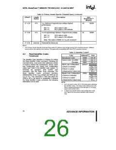
Internally, this device programs many flash cells in
parallel. Because of this parallel programming,
maximum programming performance and lower
power are obtained by aligning the start address at
the beginning of
(i.e., A4–A0 of the start address = 0).
At this point, a Read Array command can be written
to read data from blocks other than that which is
suspended. A program command sequence can
also be issued during erase suspend to program
data in other blocks. During a program operation
with block erase suspended, status register bit
SR.7 will return to “0” and the STS output (in default
a
write buffer boundary
After the final buffer data is given, a Write Confirm
command is issued. This initiates the WSM (Write
State Machine) to begin copying the buffer data to
the flash array. If a command other than Write
Confirm is written to the device, an “Invalid
Command/Sequence” error will be generated and
Status Register bits SR.5 and SR.4 will be set to a
“1.” For additional buffer writes, issue another Write
to Buffer setup command and check XSR.7.
mode) will transition to VOL
.
The only other valid commands while block erase is
suspended are Read Query, Read Status Register,
Clear Status Register, Configure, and Block Erase
Resume. After a Block Erase Resume command is
written to the flash memory, the WSM will continue
the block erase process. Status register bits SR.6
and SR.7 will automatically clear and STS (in
default mode) will return to VOL. After the Erase
Resume command is written, the device
automatically outputs status register data when
read (see Figure 10). VPEN must remain at VPENH
(the same VPEN level used for block erase) while
block erase is suspended. RP# must also remain at
VIH or VHH (the same RP# level used for block
erase). Block erase cannot resume until program
operations initiated during block erase suspend
have completed.
If an error occurs while writing, the device will stop
writing, and Status Register bit SR.4 will be set to a
“1” to indicate a program failure. The internal WSM
verify only detects errors for “1”s that do not
successfully program to “0”s. If a program error is
detected, the status register should be cleared. Any
time SR.4 and/or SR.5 is set (e.g., a media failure
occurs during a program or an erase), the device
will not accept any more Write to Buffer commands.
Additionally, if the user attempts to program past an
erase block boundary with
a Write to Buffer
command, the device will abort the Write to Buffer
operation. This will generate an "Invalid Command/
Sequence" error and Status Register bits SR.5 and
SR.4 will be set to a “1.”
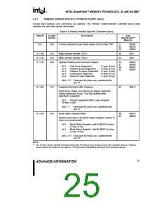
4.8
Write to Buffer Command
Reliable buffered writes can only occur when
To program the flash device, a Write to Buffer
command sequence is initiated. A variable number
of bytes, up to the buffer size, can be loaded into
the buffer and written to the flash device. First, the
Write to Buffer setup command is issued along with
the Block Address (see Figure 7, Write to Buffer
Flowchart). At this point, the eXtended Status
Register (XSR, see Table 17) information is loaded
and XSR.7 reverts to "buffer available" status. If
XSR.7 = 0, the write buffer is not available. To retry,
continue monitoring XSR.7 by issuing the Write to
Buffer setup command with the Block Address until
XSR.7 = 1. When XSR.7 transitions to a “1,” the
buffer is ready for loading.
V
PEN = VPENH. If a buffered write is attempted while
VPEN ≤ VPENLK, Status Register bits SR.4 and SR.3
will be set to “1.” Buffered write attempts with
invalid VCC and VPEN voltages produce spurious
results and should not be attempted. Finally,
successful programming requires that the
corresponding Block Lock-Bit be reset or, if set, that
RP# = VHH. If a buffered write is attempted when
the corresponding Block Lock-Bit is set and RP# =
VIH, SR.1 and SR.4 will be set to “1.” Buffered write
operations with VIH < RP# < VHH produce spurious
results and should not be attempted.
Now a word/byte count is given to the part with the
Block Address. On the next write, a device start
address is given along with the write buffer data.
Subsequent writes provide additional device
addresses and data, depending on the count. All
subsequent addresses must lie within the start
address plus the count.
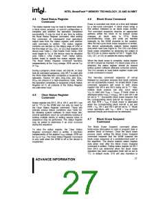
4.9
Byte/Word Program Commands
Byte/Word program is executed by a two-cycle
command sequence. Byte/Word program setup
(standard 40H or alternate 10H) is written followed
by a second write that specifies the address and
data (latched on the rising edge of WE#). The WSM
28
ADVANCE INFORMATION

 INTEL [ INTEL ]