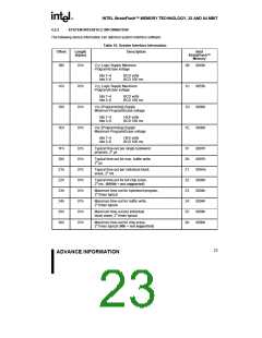
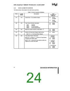
E
INTEL StrataFlash™ MEMORY TECHNOLOGY, 32 AND 64 MBIT
4.4
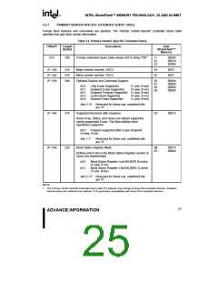
Read Status Register
Command
4.6
Block Erase Command
Erase is executed one block at a time and initiated
by a two-cycle command. A block erase setup is
first written, followed by an block erase confirm.
This command sequence requires an appropriate
address within the block to be erased (erase
changes all block data to FFH). Block
preconditioning, erase, and verify are handled
internally by the WSM (invisible to the system).
After the two-cycle block erase sequence is written,
the device automatically outputs status register
data when read (see Figure 9). The CPU can detect
block erase completion by analyzing the output of
the STS pin or status register bit SR.7. Toggle OE#,
CE0, CE1, or CE2 to update the status register.
The status register may be read to determine when
a block erase, program, or lock-bit configuration is
complete and whether the operation completed
successfully. It may be read at any time by writing
the Read Status Register command. After writing
this command, all subsequent read operations
output data from the status register until another
valid command is written. The status register
contents are latched on the falling edge of OE# or
the first edge of CE0, CE1, or CE2 that enables the
device (see Table 2, Chip Enable Truth Table). OE#
must toggle to VIH or the device must be disabled
(see Table 2, Chip Enable Truth Table) before
further reads to update the status register latch.
The Read Status Register command functions
independently of the VPEN voltage. RP# can be VIH
When the block erase is complete, status register
bit SR.5 should be checked. If a block erase error is
detected, the status register should be cleared
before system software attempts corrective actions.
The CUI remains in read status register mode until
a new command is issued.
or VHH
.
During a program, block erase, set lock-bit, or clear
lock-bit command sequence, only SR.7 is valid until
the Write State Machine completes or suspends the
operation. Device I/O pins DQ0–DQ6 and DQ8–
DQ15 are placed in a high-impedance state. When
the operation completes or suspends (check Status
Register bit 7), all contents of the Status Register
are valid when read.
This two-step command sequence of set-up
followed by execution ensures that block contents
are not accidentally erased. An invalid Block Erase
command sequence will result in both status
register bits SR.4 and SR.5 being set to “1.” Also,
reliable block erasure can only occur when
VCC is valid and VPEN = VPENH. If block erase is
attempted while VPEN ≤ VPENLK, SR.3 and SR.5 will
be set to “1.” Successful block erase requires that
the corresponding block lock-bit be cleared or, if
set, that RP# = VHH. If block erase is attempted
when the corresponding block lock-bit is set and
RP# = VIH, SR.1 and SR.5 will be set to “1.” Block
erase operations with VIH < RP# < VHH produce
spurious results and should not be attempted.
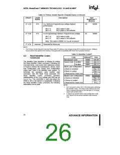
4.5
Clear Status Register
Command
Status register bits SR.5, SR.4, SR.3, and SR.1 are
set to “1”s by the WSM and can only be reset by
the Clear Status Register command. These bits
indicate various failure conditions (see Table 16).
By allowing system software to reset these bits,
several operations (such as cumulatively erasing or
locking multiple blocks or writing several bytes in
sequence) may be performed. The status register
may be polled to determine if an error occurred
during the sequence.
4.7
Block Erase Suspend
Command
The Block Erase Suspend command allows
block-erase interruption to read or program data in
another block of memory. Once the block erase
process starts, writing the Block Erase Suspend
command requests that the WSM suspend the
block erase sequence at a predetermined point in
the algorithm. The device outputs status register
data when read after the Block Erase Suspend
command is written. Polling status register bit SR.7
then SR.6 can determine when the block erase
operation has been suspended (both will be set to
“1”). In default mode, STS will also transition to
To clear the status register, the Clear Status
Register command (50H) is written. It functions
independently of the applied VPEN voltage. RP# can
be VIH or VHH. The Clear Status Register Command
is only valid when the WSM is off or the device is
suspended.
27
ADVANCE INFORMATION

 INTEL [ INTEL ]