E
INTEL StrataFlash™ MEMORY TECHNOLOGY, 32 AND 64 MBIT
3.3 Standby
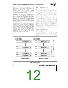
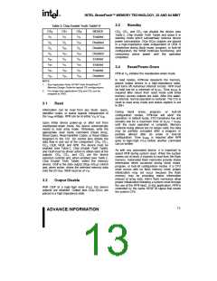
Table 2. Chip Enable Truth Table(1,2)
CE2
VIL
VIL
VIL
VIL
VIH
VIH
VIH
VIH
CE1
VIL
VIL
VIH
VIH
VIL
VIL
VIH
VIH
CE0
VIL
VIH
VIL
VIH
VIL
VIH
VIL
VIH
DEVICE
Enabled
Disabled
Disabled
Disabled
Enabled
Enabled
Enabled
Disabled
CE0, CE1, and CE2 can disable the device (see
Table 2, Chip Enable Truth Table) and place it in
standby mode which substantially reduces device
power consumption. DQ0–DQ15 outputs are placed
in a high-impedance state independent of OE#. If
deselected during block erase, program, or lock-bit
configuration, the WSM continues functioning, and
consuming active power until the operation
completes.
3.4
Reset/Power-Down
RP# at VIL initiates the reset/power-down mode.
In read modes, RP#-low deselects the memory,
places output drivers in a high-impedance state,
and turns off numerous internal circuits. RP# must
be held low for a minimum of tPLPH. Time tPHQV is
required after return from reset mode until initial
memory access outputs are valid. After this wake-
up interval, normal operation is restored. The CUI is
reset to read array mode and status register is set
to 80H.
NOTE:
1. See Application Note AP-647 Intel StrataFlash™
Memory Design Guide for typical CE configurations.
2. For single-chip applications CE2 and CE1 can be
strapped to GND.
3.1
Read
Information can be read from any block, query,
identifier codes, or status register independent of
During block erase, program, or lock-bit
configuration modes, RP#-low will abort the
operation. In default mode, STS transitions low and
remains low for a maximum time of tPLPH + tPHRH
until the reset operation is complete. Memory
contents being altered are no longer valid; the data
may be partially corrupted after a program or
partially altered after an erase or lock-bit
configuration. Time tPHWL is required after RP#
goes to logic-high (VIH) before another command
can be written.
the VPEN voltage. RP# can be at either VIH or VHH
.
Upon initial device power-up or after exit from
reset/power-down mode, the device automatically
resets to read array mode. Otherwise, write the
appropriate read mode command (Read Array,
Read Query, Read Identifier Codes, or Read Status
Register) to the CUI. Six control pins dictate the
data flow in and out of the component: CE0, CE1,
CE2, OE#, WE#, and RP#. The device must be
enabled (see Table 2, Chip Enable Truth Table),
and OE# must be driven active to obtain data at the
outputs. CE0, CE1, and CE2 are the device
selection controls and, when enabled (see Table 2,
Chip Enable Truth Table), select the memory
device. OE# is the data output (DQ0–DQ15) control
and, when active, drives the selected memory data
As with any automated device, it is important to
assert RP# during system reset. When the system
comes out of reset, it expects to read from the flash
memory. Automated flash memories provide status
information when accessed during block erase,
program, or lock-bit configuration modes. If a CPU
reset occurs with no flash memory reset, proper
initialization may not occur because the flash
memory may be providing status information
instead of array data. Intel’s flash memories allow
proper initialization following a system reset through
the use of the RP# input. In this application, RP# is
controlled by the same RESET# signal that resets
the system CPU.
onto the I/O bus. WE# must be at VIH
.
3.2
Output Disable
With OE# at a logic-high level (VIH), the device
outputs are disabled. Output pins DQ0–DQ15 are
placed in a high-impedance state.
13
ADVANCE INFORMATION

 INTEL [ INTEL ]