E
INTEL StrataFlash™ MEMORY TECHNOLOGY, 32 AND 64 MBIT
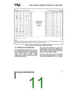
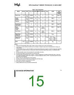
Table 3. Bus Operations
(10)
Mode
Notes RP# CE0,1,2
OE#(11)WE#(11) Address VPEN
DQ(8)
STS
(default
mode)
Read Array
1,2,3 VIH or Enabled
VHH
VIL
VIH
X
VIH
VIH
X
X
X
X
X
X
X
X
X
X
DOUT
High Z(9)
Output
Disable
VIH or Enabled
VHH
High Z
High Z
High Z
Note 4
X
Standby
VIH or Disabled
VHH
X
Reset/Power-
Down Mode
VIL
X
X
X
High Z(9)
High Z(9)
Read
V
IH or Enabled
VIL
VIH
See
Identifier
Codes
VHH
Figure 6
Read Query
VIH or Enabled
VHH
VIL
VIL
VIL
VIH
VIH
VIH
See
Table 7
X
X
Note 5
DOUT
High Z(9)
Read Status
(WSM off)
VIH or Enabled
VHH
X
X
Read Status
(WSM on)
VIH or Enabled
VHH
VPENH
DQ7 = DOUT
DQ15–8 = High Z
DQ6–0 = High Z
Write
3,6,7 VIH or Enabled
VHH
VIH
VIL
X
X
DIN
X
NOTES:
1. Refer to DC Characteristics. When VPEN ≤ VPENLK, memory contents can be read, but not altered.
2. X can be VIL or VIH for control and address pins, and VPENLK or VPENH for VPEN. See DC Characteristics for VPENLK and
PENH voltages.
V
3. In default mode, STS is VOL when the WSM is executing internal block erase, program, or lock-bit configuration algorithms.
It is VOH when the WSM is not busy, in block erase suspend mode (with programming inactive), or reset/power-down
mode.
4. See Read Identifier Codes Command section for read identifier code data.
5. See Read Query Mode Command section for read query data.
6. Command writes involving block erase, program, or lock-bit configuration are reliably executed when VPEN = VPENH and
V
CC is within specification. Block erase, program, or lock-bit configuration with VIH < RP# < VHH produce spurious results
and should not be attempted.
7. Refer to Table 4 for valid DIN during a write operation.
8. DQ refers to DQ0–DQ7 if BYTE# is low and DQ0–DQ15 if BYTE# is high.
9. High Z will be VOH with an external pull-up resistor.
10. See Table 2 for valid CE configurations.
11. OE# and WE# should never be enabled simultaneously.
15
ADVANCE INFORMATION

 INTEL [ INTEL ]