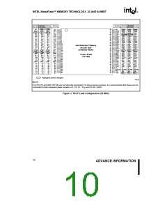
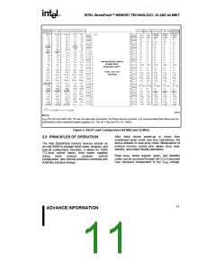
INTEL StrataFlash™ MEMORY TECHNOLOGY, 32 AND 64 MBIT
E
VPEN additionally enables block erase, program,
and lock-bit configuration operations.
3.5
Read Query
The read query operation outputs block status
information, CFI (Common Flash Interface) ID
string, system interface information, device
geometry information, and Intel-specific extended
query information.
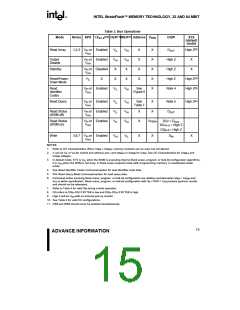
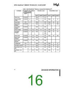
Device operations are selected by writing specific
commands into the CUI. Table 4 defines these
commands.
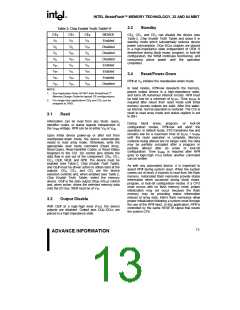
Word
Address
A[22-1]: 64 Mbit
A[21-1]: 32 Mbit
3.6
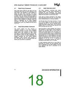
Read Identifier Codes
3FFFFF
Block 63
The read identifier codes operation outputs the
manufacturer code, device code, block lock
configuration codes for each block, and the master
lock configuration code (see Figure 6). Using the
manufacturer and device codes, the system CPU
can automatically match the device with its proper
algorithms. The block lock and master lock
configuration codes identify locked and unlocked
blocks and master lock-bit setting.
Reserved for Future
Implementation
3F0003
3F0002
Block 63 Lock Configuration
Reserved for Future
Implementation
3F0000
3EFFFF
(Blocks 32 through 62)
Block 31
Reserved for Future
Implementation
3.7
Write
Writing commands to the CUI enables reading of
device data, query, identifier codes, inspection and
1F0003
1F0002
Block 31 Lock Configuration
clearing of the status register, and, when VPEN
VPENH block erasure, program, and lock-bit
configuration.
=
Reserved for Future
Implementation
,
1F0000
1EFFFF
(Blocks 2 through 30)
The Block Erase command requires appropriate
command data and an address within the block to
be erased. The Byte/Word Program command
requires the command and address of the location
to be written. Set Master and Block Lock-Bit
commands require the command and address
within the device (Master Lock) or block within the
device (Block Lock) to be locked. The Clear Block
Lock-Bits command requires the command and
address within the device.
01FFFF
Block 1
Reserved for Future
Implementation
010003
010002
Block 1 Lock Configuration
Reserved for Future
Implementation
010000
00FFFF
Block 0
Reserved for Future
Implementation
The CUI does not occupy an addressable memory
location. It is written when the device is enabled
and WE# is active. The address and data needed to
execute a command are latched on the rising edge
of WE# or the first edge of CE0, CE1, or CE2 that
disables the device (see Table 2, Chip Enable Truth
Table). Standard microprocessor write timings are
used.
000004
000003
Master Lock Configuration
Block 0 Lock Configuration
Device Code
000002
000001
000000
Manufacturer Code
0606_06
NOTE:
4.0 COMMAND DEFINITIONS
A0 is not used in either x8 or x16 modes when obtaining
these identifier codes. Data is always given on the low byte
in x16 mode (upper byte contains 00h).
When the VPEN voltage
≤ VPENLK, only read
operations from the status register, query, identifier
codes, or blocks are enabled. Placing VPENH on
Figure 6. Device Identifier Code Memory Map
14
ADVANCE INFORMATION

 INTEL [ INTEL ]