Ultra-Low Voltage Intel® Celeron® Processor — 650 MHz and 400 MHz
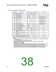
Table 28. TAP Signal AC Specifications
Symbol
Parameter
TCK Frequency
Min
Max
Unit
Figure
Notes1
T30
T31
T32
T33
—
60
16.67 MHz
TCK Period
—
ns
ns
ns
TCK High Time
TCK Low Time
25.0
25.0
≥ VCMOSREF+0.2 V, 2
≤ VCMOSREF-0.2 V, 2
(VCMOSREF-0.2 V) –
T34
T35
TCK Rise Time
TCK Fall Time
5.0
5.0
ns
ns
(VCMOSREF+0.2 V), 2, 3
(VCMOSREF+0.2 V) –
(VCMOSREF-0.2 V), 2, 3
T36
T37
T38
T39
T40
TRST# Pulse Width
TDI, TMS Setup Time
TDI, TMS Hold Time
TDO Valid Delay
40.0
5.0
ns
ns
ns
ns
ns
14
13
13
13
13
Asynchronous, 2
4
4
14.0
1.0
10.0
25.0
5, 6
2, 5, 6
TDO Float Delay
All Non-Test Outputs Valid
Delay
T41
T42
2.0
25.0
25.0
ns
ns
13
13
5, 7, 8
All Non-Test Outputs Float
Delay
2, 5, 7, 8
T43
T44
All Non-Test Inputs Setup Time
All Non-Test Inputs Hold Time
5.0
ns
ns
13
13
4, 7, 8
4, 7, 8
13.0
NOTES:
1. All AC timings for TAP signals are referenced to the TCK rising edge at 1.0 V. All TAP and CMOS signals
are referenced at 1.0 V.
2. Not 100% tested. Specified by design/characterization.
3. 1 ns may be added to the maximum TCK rise and fall times for every 1 MHz below 16 MHz.
4. Referenced to TCK rising edge.
5. Referenced to TCK falling edge.
6. Valid delay timing for this signal is specified into 150 Ω terminated to 1.5 V and 0 pF of external load. For
real system timings these specifications must be derated for external capacitance at 105 ps/pF.
7. Non-Test Outputs and Inputs are the normal output or input signals (except TCK, TRST#, TDI, TDO, and
TMS). These timings correspond to the response of these signals due to boundary scan operations.
8. During Debug Port operation use the normal specified timings rather than the TAP signal timings.
38
Datasheet

 INTEL [ INTEL ]